

Philips tda5636b, tda56 37b DATASHEETS

INTEGRATED CIRCUITS
DATA SH EET
TDA5636B; TDA5637B
9 V VHF hyperband and UHF
mixer/oscillator for TV and VCR
3-band tuners
Product specification
Supersedes data of 1995 August 01
File under Integrated Circuits, IC02
1996 Dec 02

Philips Semiconductors Product specification
9 V VHF hyperband and UHF
mixer/oscillator for TV and VCR 3-band
TDA5636B; TDA5637B
FEATURES
• Balanced mixer with a common emitter input for band A
(single input)
• 2-pin oscillator for bands A and B
• Balanced mixer with a common base input for bands B
and C (balanced input)
• 4-pin oscillator for band C
• Local oscillator buffer output for external prescaler
• SAW filter preamplifier with a low output impedance to
drive the SAW filter directly
• Band gap voltage stabilizer for oscillator stability
• Electronic band switch
• External IF filter between the mixer output and the IF
amplifier input
• Pin-to-pin compatible with TDA5636; TDA5637 family
(same function with asymmetrical IF output).
APPLICATIONS
• 3-band all channel TV and VCR tuners
• Any standard.
GENERAL DESCRIPTION
The TDA5636B and TDA5637B are monolithic integrated
circuits that perform the mixer/oscillator functions for
bands A, B and C in TV and VCR tuners. These low-power
mixer/oscillators require a power supply of 9 V and are
available in a very small package.
The devices give the designer the capability to design an
economical and physically small 3-band tuner.
They are suitable for European standards, as illustrated in
Fig.17, with the following RF bands:
• 48.25 to 168.25 MHz
• 175.25 to 447.25 MHz
• 455.25 to 855.25 MHz.
With an appropriate tuned circuit, they are also suitable for
NTSC all channel tuners (USA and Japan). The tuner
development time can be drastically reduced by using
these devices.
These circuits belong to the TDA5636/TDA5737 family
which has exactly the same function with an IF amplifier
having an asymmetrical IF output to drive a 75 Ω load. It is
possible to build tuners with either an asymmetrical or a
symmetrical IF output with one main tuner lay-out.
1996 Dec 02 2
Philips Semiconductors Product specification
9 V VHF hyperband and UHF mixer/oscillator
TDA5636B; TDA5637B
for TV and VCR 3-band tuners
QUICK REFERENCE DATA
SYMBOL PARAMETER CONDITIONS MIN. TYP. MAX. UNIT
V
P
I
P
f
RF
G
v
NF noise figure band A − 7.5 − dB
V
o
supply voltage − 9.0 − V
supply current band A − 43 − mA
band B − 39 − mA
band C − 42 − mA
frequency range RF input; band A; note 1 45 − 180 MHz
RF input; band B; note 1 160 − 470 MHz
RF input; band C; note 1 430 − 860 MHz
voltage gain band A − 25 − dB
band B − 36 − dB
band C − 36 − dB
band B − 6 − dB
band C − 7 − dB
output voltage to get 1% cross
modulation in channel
band A − 121 − dBµV
band B − 120 − dBµV
band C − 119 − dBµV
Note
1. The limits are related to the tank circuits used in Fig.17 and the intermediate frequency. Frequency bands may be
adjusted by the choice of external components.
ORDERING INFORMATION
TYPE
NUMBER
TDA5636BT
NAME DESCRIPTION VERSION
(1)
SO24
TDA5636BM SSOP24
TDA5637BT SO24
TDA5637BM SSOP24
plastic small outline package; 24 leads; body width 7.5 mm
plastic shrink small outline package; 24 leads; body width 5.3 mm
plastic small outline package; 24 leads; body width 7.5 mm
plastic shrink small outline package; 24 leads; body width 5.3 mm
PACKAGE
SOT137-1
SOT340-1
SOT137-1
SOT340-1
Note
1. The TDA5636BT is available on request.
1996 Dec 02 3
Philips Semiconductors Product specification
9 V VHF hyperband and UHF
mixer/oscillator for TV and VCR 3-band
TDA5636B; TDA5637B
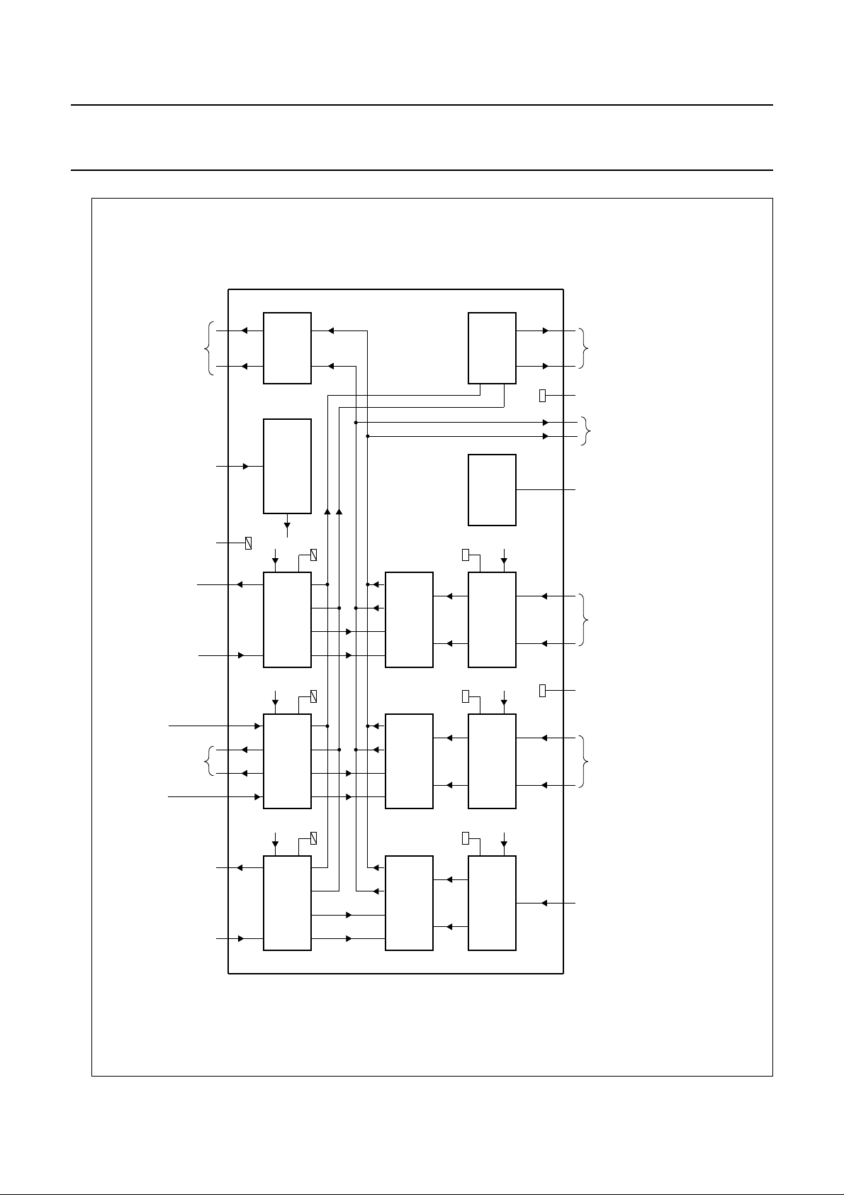
IF outputs
input
band switch
GND2
tuned circuit
band B oscillator
tuned circuit
band B oscillator
tuned circuit
band C oscillator
band C
oscillator
tuned circuit
13
(12)
(11)
(10)
(9)
(8)
(6)
(7)
(5)
(4)
(2)
IF
AMPLIFIER
ELECTRONIC
BAND SWITCH
BAND B
OSCILLATOR
BAND C
OSCILLATOR
TDA5636B
TDA5637B
MIXERMIXERMIXER
LOCAL
AMPLIFIER
OSCILLATOR
DC
STABILIZER
STAGE
BAND B
STAGE
BAND C
14
15
16
17
19
18
20
21
23
MGC504
12
(13)
11
(14)
local oscillator
10
(15)
9
(16)
8
(17)
7
(18)
5
(20)
4
(21)
3
(22)
2
(23)
1
(24)
amplifier output
GND1
mixers output
P
band B input
RF
GND
band C input
handbook, full pagewidth
Fig.1 Block diagram.
tuned circuit
band C oscillator
22
(3)
tuned circuit
band A oscillator
(1)
BAND A
OSCILLATOR
24
tuned circuit
band A oscillator
BLOCK DIAGRAM
1996 Dec 02 4
STAGE
BAND A
6
(19)
band A input V
The numbers given in parenthesis represent the TDA5637B.
The TDA5636B and TDA5637B are pin compatible with the TDA5636 and TDA5637 respectively.

Philips Semiconductors Product specification
9 V VHF hyperband and UHF mixer/oscillator
TDA5636B; TDA5637B
for TV and VCR 3-band tuners
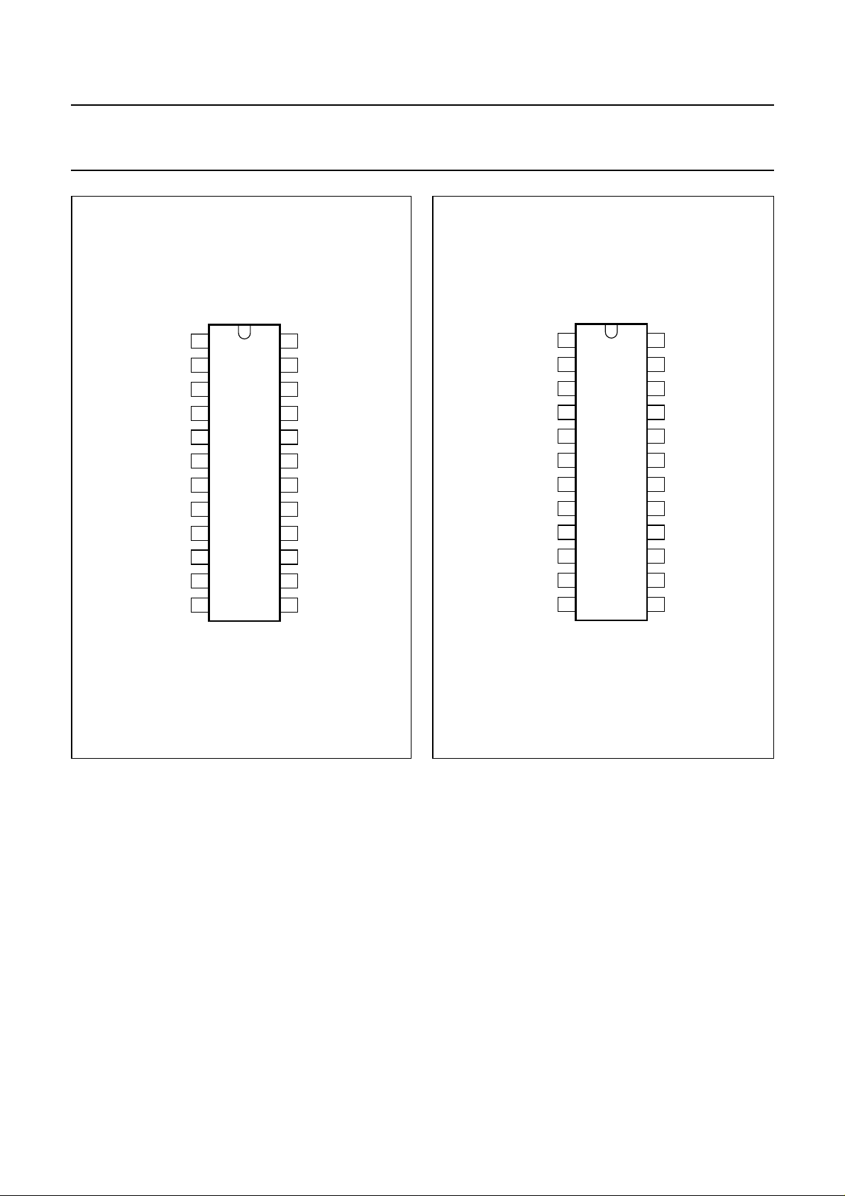
PINNING
SYMBOL
CIN1 1 24 band C input 1
CIN2 2 23 band C input 2
RFGND 3 22 ground for RF inputs
BIN1 4 21 band B input 1
BIN2 5 20 band B input 2
AIN 6 19 band A input
V
P
MIXOUT1 8 17 mixers output 1
MIXOUT2 9 16 mixers output 2
GND1 10 15 ground 1 (0 V)
LOOUT1 11 14 local oscillator amplifier output 1
LOOUT2 12 13 local oscillator amplifier output 2
IFOUT1 13 12 IF amplifier output 1
IFOUT2 14 11 IF amplifier output 2
BS 15 10 electronic band switch input
GND2 16 9 ground 2 (0 V)
BOSCOC 17 8 band B oscillator output collector
COSCIB1 18 7 band C oscillator input base 1
BOSCIB 19 6 band B oscillator input base
COSCOC1 20 5 band C oscillator output collector 1
COSCOC2 21 4 band C oscillator output collector 2
AOSCOC 22 3 band A oscillator output collector
COSCIB2 23 2 band C oscillator input base 2
AOSCIB 24 1 band A oscillator input base
TDA5636B TDA5637B
PIN
DESCRIPTION
7 18 supply voltage
1996 Dec 02 5
Philips Semiconductors Product specification
9 V VHF hyperband and UHF mixer/oscillator
for TV and VCR 3-band tuners
handbook, halfpage
MIXOUT1
MIXOUT2
1
CIN1 AOSCIB
2
CIN2
BIN1
BIN2
AIN
V
GND1
P
3
4
5
6
TDA5636B
7
8
9
10
11
12
RFGND
LOOUT1
LOOUT2
24
23
22
21
20
19
18
17
16
15
14
13
MGC502
COSCIB2
AOSCOC
COSCOC2
COSCOC1
BOSCIB
COSCIB1
BOSCOC
GND2
BS
IFOUT2
IFOUT1
handbook, halfpage
TDA5636B; TDA5637B
AOSCIB CIN1
COSCIB2
AOSCOC
COSCOC2
COSCOC1
BOSCIB
1
2
3
4
5
6
TDA5637B
GND2
BS
7
8
9
10
11
12
COSCIB1
BOSCOC
IFOUT2
IFOUT1
24
23
22
21
20
19
18
17
16
15
14
13
MGC503
CIN2
RFGND
BIN1
BIN2
AIN
V
P
MIXOUT1
MIXOUT2
GND1
LOOUT1
LOOUT2
Fig.2 Pin configuration (TDA5636B).
1996 Dec 02 6
Fig.3 Pin configuration (TDA5637B).
Philips Semiconductors Product specification
9 V VHF hyperband and UHF mixer/oscillator
TDA5636B; TDA5637B
for TV and VCR 3-band tuners
LIMITING VALUES
In accordance with the Absolute Maximum Rating System (IEC 134).
SYMBOL PARAMETER MIN. MAX. UNIT
V
P
V
SW
I
O
t
sc(max)
T
stg
T
amb
T
j
HANDLING
Human Body Model:
• For TDA5636B GND (10) (16), RFGND (3), and V
• For TDA5637B GND (9) (15), RFGND (22), and VP(18) are separate.
All pins withstand 2000 V in accordance with the
category B (2000 V); R = 1500 Ω; C = 100 pF.
supply voltage −0.3 +10.5 V
switching voltage 0 +10.5 V
output current of each pin to ground −−10 mA
maximum short-circuit time (all pins) − 10 s
IC storage temperature −55 +150 °C
operating ambient temperature −10 +80 °C
junction temperature − +150 °C
(7) are separate.
P
“UZW-B0/FQ-A302”
specification equivalent to the
“MIL-STD-883C”
Machine Model:
• For TDA5636B GND (10) (16), RFGND (3), and VP(7) are separate.
• For TDA5637B GND (9) (15), RFGND (22), and VP(18) are separate.
All pins withstand 175 V in accordance with the
“UZW-B0/FQ-A302”
specification (date of issue: Nov 6th, 1990); R = 0 Ω;
C = 200 pF.
THERMAL CHARACTERISTICS
SYMBOL PARAMETER VALUE UNIT
R
th j-a
thermal resistance from junction to ambient in free air
SSOP24 120 K/W
SO24 75 K/W
1996 Dec 02 7
Philips Semiconductors Product specification
9 V VHF hyperband and UHF mixer/oscillator
TDA5636B; TDA5637B
for TV and VCR 3-band tuners
CHARACTERISTICS
=9V; T
V
P
SYMBOL PARAMETER CONDITIONS MIN. TYP. MAX. UNIT
Supply
V
P
I
P
V
SW
I
SW
Band A mixer (including IF amplifier)
f
RF
G
v
NF noise figure f
V
o
V
i
g
os
Y
i
C
i
Band A oscillator
f
OSC
f
shift
f
drift
=25°C; measured in circuit of Fig.17; unless otherwise specified.
amb
supply voltage 8.1 9.0 9.9 V
supply current band A − 43 48 mA
band B − 39 44 mA
band C − 42 47 mA
switching voltage band A 0 − 1.1 V
band B 1.6 − 2.4 V
band C 3.0 − V
V
P
switching current band A −−2µA
band B −−5µA
band C; V
=5V −−10 µA
SW(C)
RF frequency note 1 45 − 180 MHz
voltage gain f
output voltage 1% cross modulation in channel;
50 MHz; see Fig.4; note 2 22.5 25.0 27.5 dB
RF =
f
180 MHz; see Fig.4; note 2 22.5 25.0 27.5 dB
RF =
= 50 MHz; see Figs 5 and 6 − 7.5 9.5 dB
RF
f
= 180 MHz; see Figs 5 and 6 − 7.5 9.5 dB
RF
118 121 − dBµV
fRF= 50 MHz; see Fig.7
1% cross modulation in channel;
f
= 180 MHz; see Fig.7
RF
input voltage 10 kHz pulling in channel;
119 122 − dBµV
− 104 − dBµV
fRF= 180 MHz; note 3
optimum source
conductance
fRF= 50 MHz − 0.5 − mS
= 180 MHz − 1 − mS
f
RF
input admittance see Fig.12 −−−mS
input capacitance fRF= 50 to 180 MHz; see Fig.12 − 2 − pF
oscillator frequency note 4 80 − 216 MHz
frequency shift ∆Vp= 10%; note 5 −−200 kHz
frequency drift ∆T=25°C with no compensation; NP0
−−600 kHz
capacitors; note 6
5 s to 15 min after switch on; note 7 −−200 kHz
1996 Dec 02 8
Philips Semiconductors Product specification
9 V VHF hyperband and UHF mixer/oscillator
TDA5636B; TDA5637B
for TV and VCR 3-band tuners
SYMBOL PARAMETER CONDITIONS MIN. TYP. MAX. UNIT
Band B mixer (including IF amplifier)
f
RF
G
v
NF noise figure
V
o
V
i
Z
i
Band B oscillator
f
OSC
f
shift
f
drift
RF frequency note 1 160 − 470 MHz
voltage gain fRF= 170 MHz; see Fig.8; note 2 33 36 39 dB
f
= 470 MHz; see Fig.8; note 2 33 36 39 dB
RF
f
= 170 MHz; see Fig.9 − 6.0 8.0 dB
RF
(not corrected for image)
output voltage 1% cross modulation in channel;
= 470 MHz; see Fig.9 − 7.0 9.0 dB
f
RF
118 121 − dBµV
fRF= 170 MHz; see Fig.10
1% cross modulation in channel;
f
= 470 MHz; see Fig.10
RF
input voltage 10 kHz pulling in channel;
117 120 − dBµV
− 91 − dBµV
fRF= 470 MHz; note 3
input voltage N+5−1 MHz pulling; f
= 430 MHz; see
RF
− 77 − dBµV
Fig.11
input impedance (Rs+jLsω)fRF= 170 to 470 MHz; see Fig.13 − 30 −Ω
f
= 170 to 470 MHz; see Fig.13 − 10 − nH
RF
oscillator frequency note 4 200 − 500 MHz
frequency shift ∆VP= 10%; note 5 −−400 kHz
frequency drift ∆T=25°C with no compensation; NP0
−−2 MHz
capacitors; note 6
5 s to 15 min. after switch on; note 7 −−300 kHz
Band C mixer (including IF amplifier)
f
RF
G
v
RF frequency note 1 430 − 860 MHz
voltage gain fRF= 430 MHz; see Fig.8; note 2 33 36 39 dB
NF noise figure
(not corrected for image)
V
o
V
i
output voltage 1% cross modulation in channel;
input voltage 10 kHz pulling in channel;
input voltage N+5−1 MHz pulling; f
Z
i
input impedance
(Rs+jLsω)
f
= 860 MHz; see Fig.8; note 2 33 36 39 dB
RF
f
= 430 MHz; see Fig.9 − 7.0 9.0 dB
RF
= 860 MHz; see Fig.9 − 8.0 10.0 dB
f
RF
116 119 − dBµV
fRF= 430 MHz; see Fig.10
1% cross modulation in channel;
f
= 860 MHz; see Fig.10
RF
116 119 − dBµV
− 103 − dBµV
fRF= 860 MHz; note 3
= 820 MHz;
RF
− 79 − dBµV
see Fig.11
fRF= 430 to 860 MHz; see Fig.14 − 40 −Ω
= 430 to 860 MHz; see Fig.14 − 10 − nH
f
RF
1996 Dec 02 9
 Loading...