

Philips tda5630, tda56 31 DATASHEETS

INTEGRATED CIRCUITS
DATA SH EET
TDA5630; TDA5631
9 V VHF, hyperband and UHF
mixer/oscillator for TV and VCR
3-band tuners
Product specification
File under Integrated Circuits, IC02
1996 Mar 21

Philips Semiconductors Product specification
9 V VHF, hyperband and UHF
mixer/oscillator for TV and VCR 3-band tuners
FEATURES
• Balanced mixer with a common emitter input for band A
(single input)
• 2-pin oscillator for bands A and B
• Balanced mixer with a common base input for
bands B and C (balanced input)
• 3-pin oscillator for band C
• Local oscillator buffer output for external synthesizer
• SAW filter preamplifier with a low output impedance to
drive the SAW filter directly
• Band gap voltage stabilizer for oscillator stability
• Electronic band switch.
APPLICATIONS
• 3-band all channel TV and VCR tuners
• Any standard.
GENERAL DESCRIPTION
The TDA5630 and TDA5631 are monolithic integrated
circuits that perform the mixer/oscillator functions for
bands A, B and C in TV and VCR tuners. These low-power
mixer/oscillators require a power supply of 9 V and are
available in a very small package.
The devices give the designer the capability to design an
economical and physically small 3-band tuner.
They are suitable for European standards, as illustrated in
Fig.12, with the following RF bands: 48.25 to 168.25 MHz,
175.25 to 447.25 MHz and 455.25 to 855.25 MHz. With
an appropriate tuned circuit, they are also suitable for
NTSC all channel tuners (USA and Japan).
The tuner development time can be drastically reduced by
using these devices.
TDA5630;
TDA5631
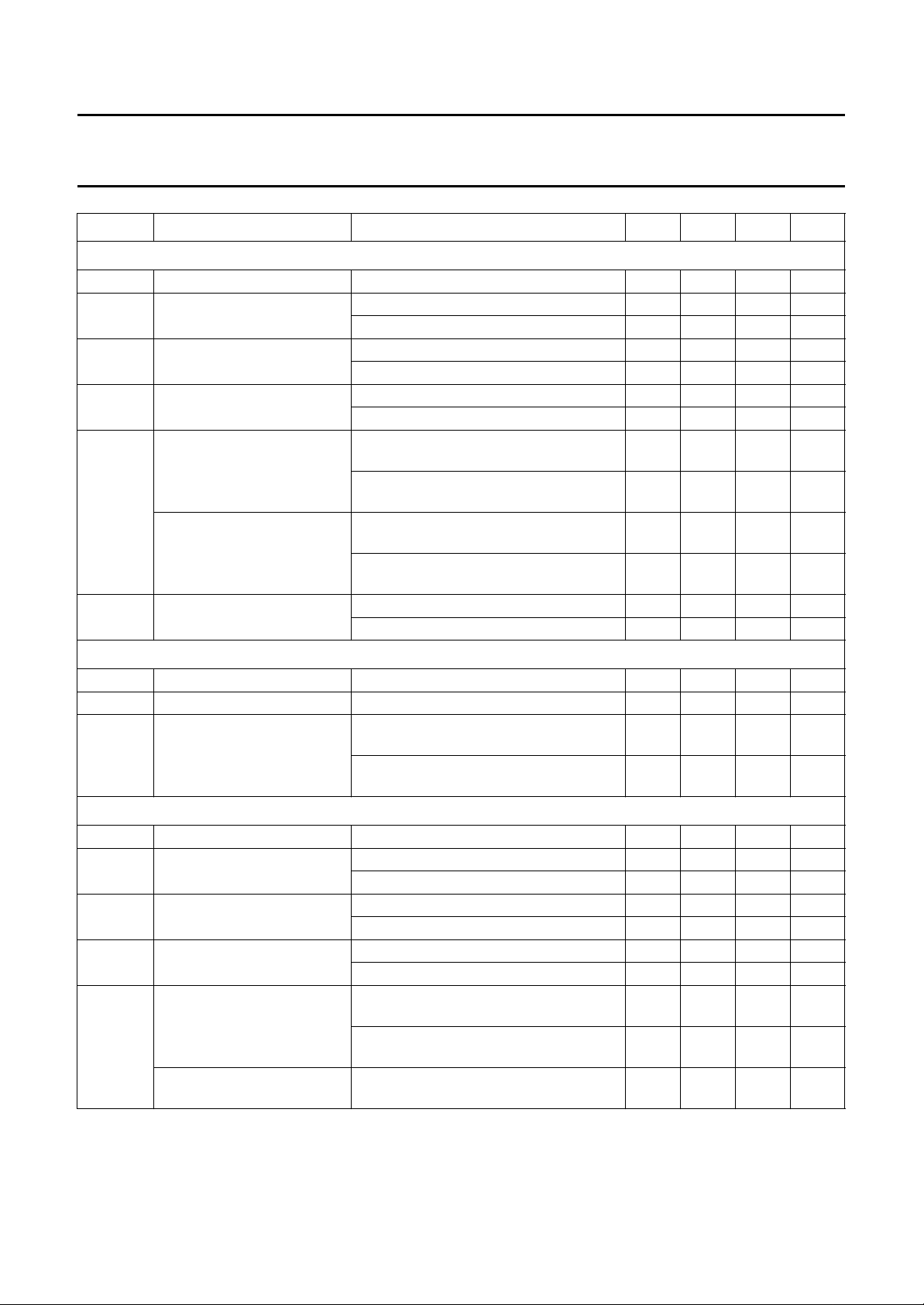
QUICK REFERENCE DATA
SYMBOL PARAMETER CONDITIONS MIN. TYP. MAX. UNIT
V
P
I
P
f
RF
G
v
NF noise figure band A − 7.5 − dB
V
o
Note
1. The limits are related to the tank circuits used in Fig.12 and the intermediate frequency. Frequency bands may be
adjusted by the choice of external components.
supply voltage − 9.0 − V
supply current − 35 − mA
frequency range RF input; band A; note 1 45 − 180 MHz
RF input; band B; note 1 160 − 470 MHz
RF input; band C; note 1 430 − 860 MHz
voltage gain band A − 25 − dB
band B − 36 − dB
band C − 36 − dB
band B − 8 − dB
band C − 9 − dB
output voltage to get 1% cross
modulation in channel
band A − 118 − dBµV
band B − 118 − dBµV
band C − 118 − dBµV
1996 Mar 21 2
Philips Semiconductors Product specification
9 V VHF, hyperband and UHF
mixer/oscillator for TV and VCR 3-band tuners
ORDERING INFORMATION
TYPE
NUMBER
NAME DESCRIPTION VERSION
TDA5630T SO20
TDA5630M SSOP20
TDA5631T SO20
TDA5631M SSOP20
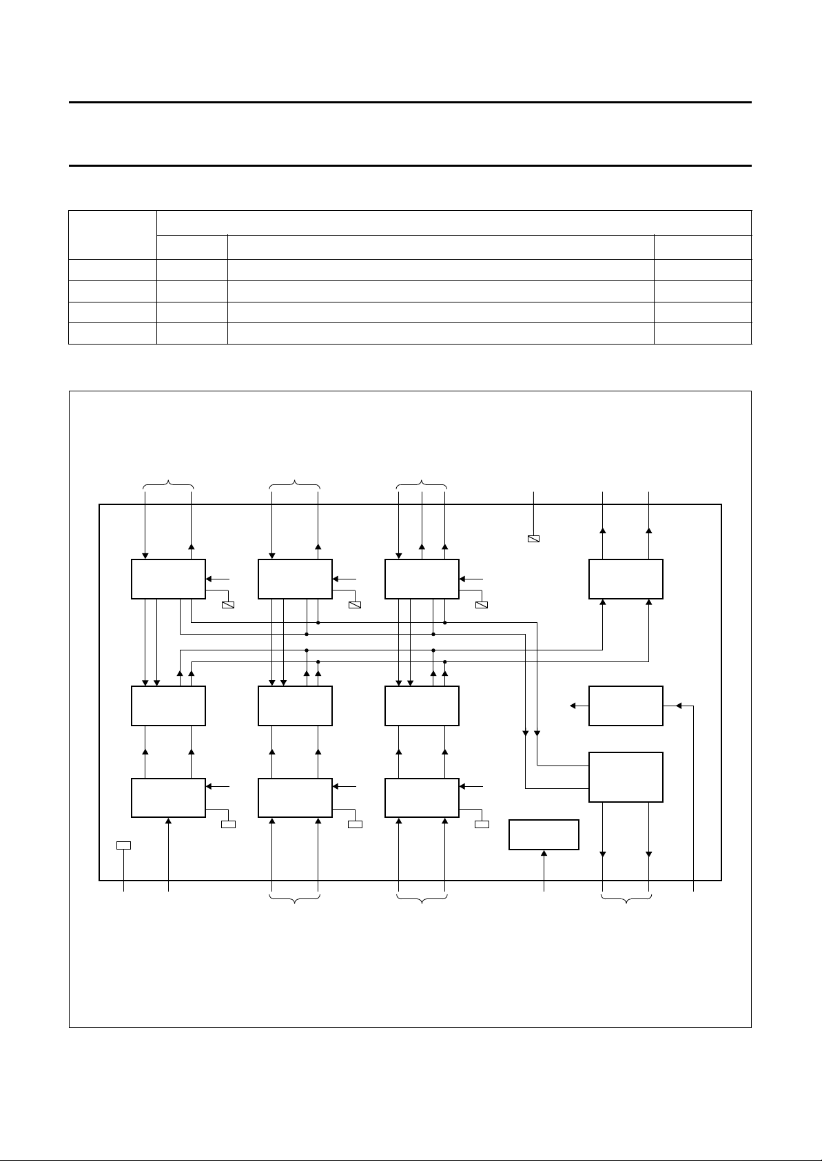
BLOCK DIAGRAM
handbook, full pagewidth
band A oscillator
tuned circuit
20
(1)
plastic small outline package; 20 leads; body width 7.5 mm
plastic shrink small outline package; 20 leads; body width 4.4 mm
plastic small outline package; 20 leads; body width 7.5 mm
plastic shrink small outline package; 20 leads; body width 4.4 mm
band B oscillator
tuned circuit
18
(3)
16
(5)
14
(7)
PACKAGE
band C oscillator
tuned circuit
19
17
(2)
(4)
15
(6)
GND
13
(8)
IF outputs
12
(9)
TDA5630;
TDA5631
SOT163-1
SOT266-1
SOT163-1
SOT266-1
MBH044
11
(10)
BAND A
OSCILLATOR
MIXER
BAND A
STAGE
input
(15)
6
(18)
3
RF GND band A
The numbers given in parenthesis represent the TDA5631.
BAND B
OSCILLATOR
MIXER MIXER
BAND B
STAGE
(16)
5
band B
inputs
(17)
4
BAND C
OSCILLATOR
BAND C
STAGE
(19)
2
band C
inputs
(20)
1
TDA5630
TDA5631
DC
STABILIZER
(14)
7
V
P
IF AMPLIFIER
ELECTRONIC
BAND
SWITCH
LOCAL
OSCILLATOR
AMPLIFIER
(13)
8
local oscillator
amplifier outputs
(12)
9
band switch
input
(11)
10
Fig.1 Block diagram.
1996 Mar 21 3
Philips Semiconductors Product specification
9 V VHF, hyperband and UHF
mixer/oscillator for TV and VCR 3-band tuners
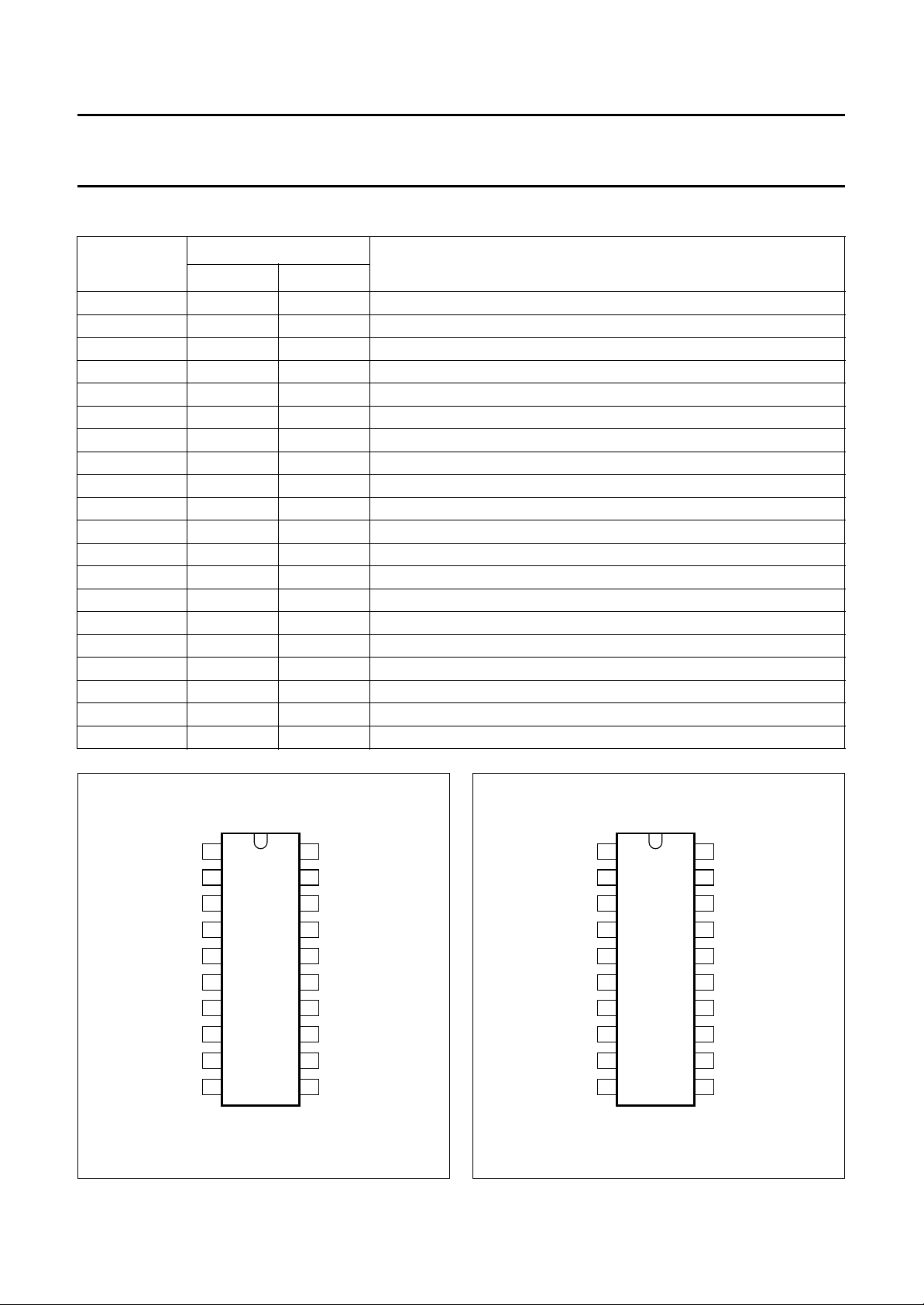
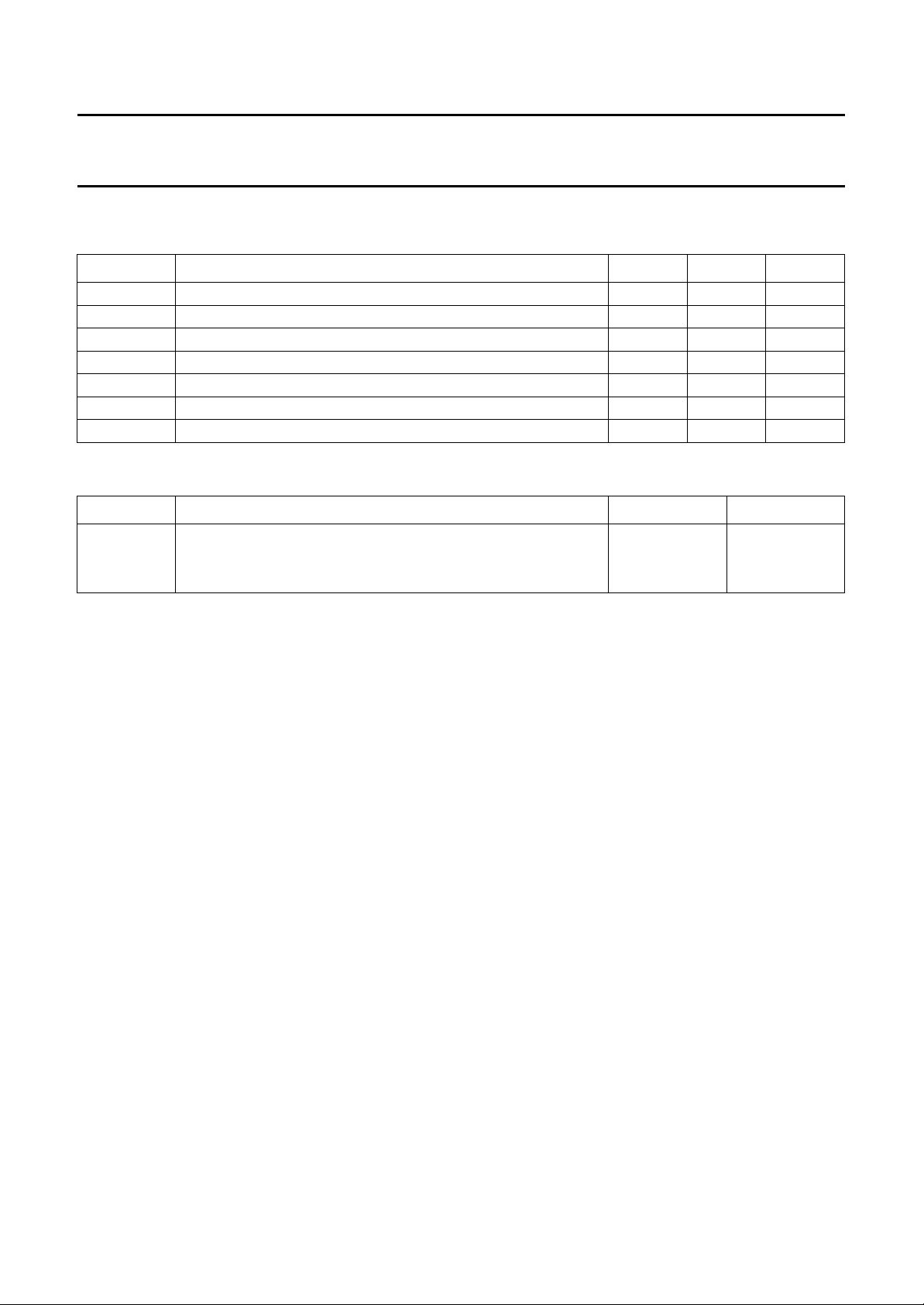
PINNING
SYMBOL
TDA5630 TDA5631
CIN1 1 20 band C input 1
CIN2 2 19 band C input 2
RFGND 3 18 ground for RF inputs
BIN1 4 17 band B input 1
BIN2 5 16 band B input 2
AIN 6 15 band A input
V
P
LOOUT1 8 13 local oscillator amplifier output 1
LOOUT2 9 12 local oscillator amplifier output 2
BS 10 11 band switch input
IFOUT1 11 10 IF amplifier output 1
IFOUT2 12 9 IF amplifier output 2
GND 13 8 ground (0 V)
BOSCOC 14 7 band B oscillator output collector
COSCOC1 15 6 band C oscillator output collector 1
BOSCIB 16 5 band B oscillator input base
COSCOC2 17 4 band C oscillator output collector 2
AOSCOC 18 3 band A oscillator output collector
COSCIB 19 2 band C oscillator input base
AOSCIB 20 1 band A oscillator input base
PIN
DESCRIPTION
7 14 supply voltage
TDA5630;
TDA5631
handbook, halfpage
RFGND
LOOUT1
LOOUT2
CIN1
CIN2
BIN1
BIN2
AIN
V
BS
P
1
2
3
4
5
6
7
8
9
10
TDA5630
MGD265
20
AOSCIB
19
COSCIB
18
AOSCOC
17
COSCOC2
16
BOSCIB
15
COSCOC1
14
BOSCOC
13
GND
12
IFOUT2
11
IFOUT1
Fig.2 Pin configuration (TDA5630).
1996 Mar 21 4
handbook, halfpage
AOSCOC
COSCOC2
COSCOC1
BOSCOC
Fig.3 Pin configuration (TDA5631).
AOSCIB
COSCIB
BOSCIB
GND
IFOUT2
IFOUT1
1
2
3
4
5
6
7
8
9
10
TDA5631
MGD266
20
19
18
17
16
15
14
13
12
11
CIN1
CIN2
RFGND
BIN1
BIN2
AIN
V
P
LOOUT1
LOOUT2
BS
Philips Semiconductors Product specification
9 V VHF, hyperband and UHF
mixer/oscillator for TV and VCR 3-band tuners
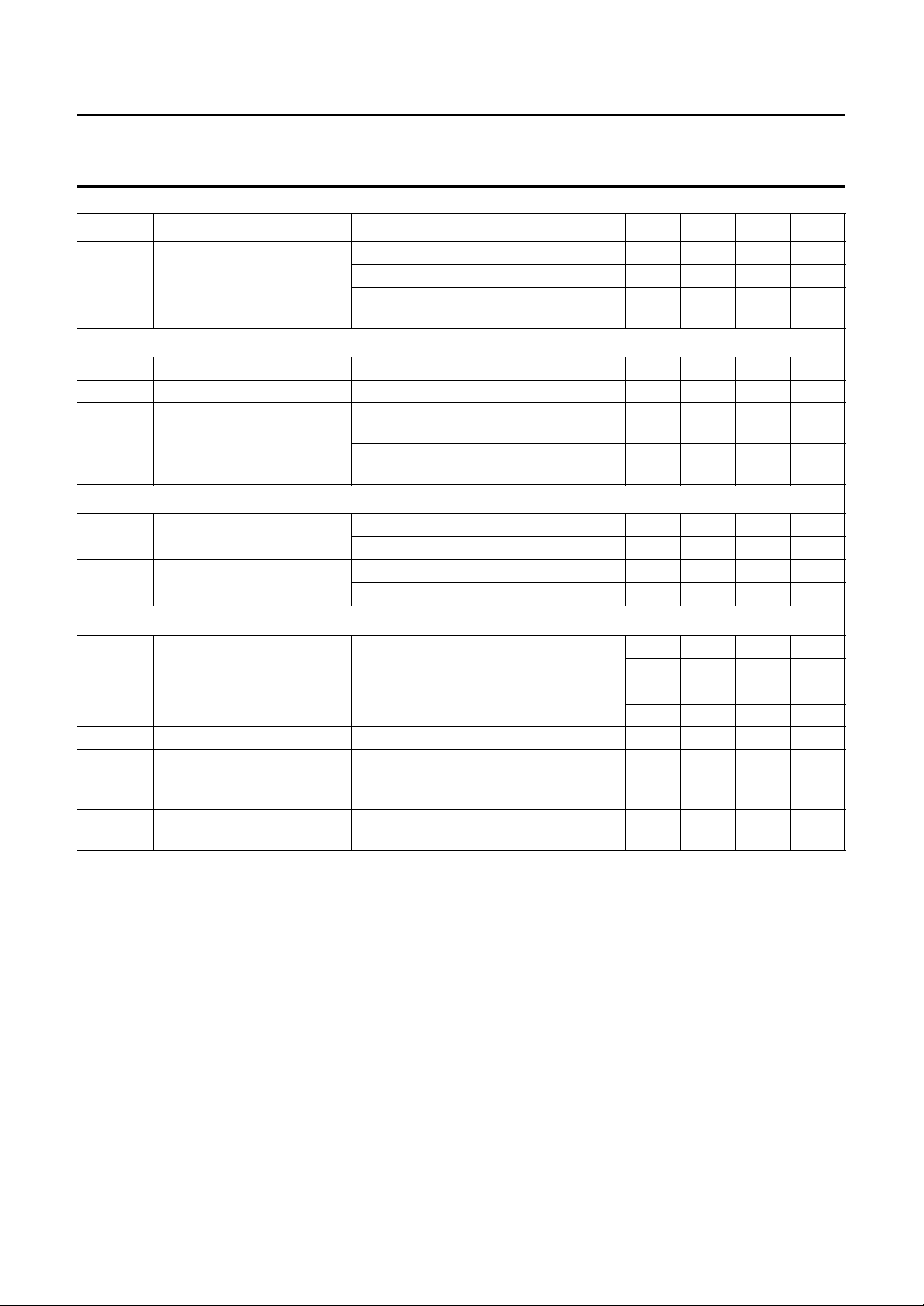
LIMITING VALUES
In accordance with the Absolute Maximum Rating System (IEC 134).
SYMBOL PARAMETER MIN. MAX. UNIT
V
P
V
SW
I
O
t
sc
T
stg
T
amb
T
j
THERMAL CHARACTERISTICS
SYMBOL PARAMETER VALUE UNIT
R
th j-a
supply voltage −0.3 +10.5 V
switching voltage 0 10.5 V
output current of each pin referenced to ground −−10 mA
maximum short-circuit time (all pins) − 10 s
IC storage temperature −55 +150 °C
operating ambient temperature −10 +80 °C
junction temperature − +150 °C
thermal resistance from junction to ambient in free air
SOT163-1 100 K/W
SOT266-1 120 K/W
TDA5630;
TDA5631
HANDLING
Human body model: the IC withstands 2000 V in accordance with the MIL-STD-883C category B (stress reference
pins 3, 7 and 13 shorted together for the TDA5630; pins 18, 14 and 8 for the TDA5631).
Machine model: the IC withstands 200 V in accordance with the MIL-STD-883C (stress reference pins 3, 7 and 13
shorted together for the TDA5630; pins 18, 14 and 8 for the TDA5631).
1996 Mar 21 5
Philips Semiconductors Product specification
9 V VHF, hyperband and UHF
mixer/oscillator for TV and VCR 3-band tuners
TDA5630;
TDA5631
CHARACTERISTICS
V
=9V; T
P
=25°C; measured in circuit of Fig.12; unless otherwise specified.
amb
SYMBOL PARAMETER CONDITIONS MIN. TYP. MAX. UNIT
Supply
V
P
I
P
V
SW
supply voltage 8.1 9.0 9.9 V
supply current − 35 45 mA
switching voltage band A 0 − 1.1 V
band B 1.6 − 2.4 V
band C 3.0 − 5.0 V
I
SW
switching current band A −−2µA
band B −−5µA
band C −−10 µA
Band A mixer including IF amplifier
f
RF
G
v
NF noise figure f
V
o
frequency range note 1 45 − 180 MHz
voltage gain fRF= 50 MHz; see Fig.4; note 2 22.5 25 27.5 dB
= 180 MHz; see Fig.4; note 2 22.5 25 27.5 dB
f
RF
= 50 MHz; see Figs 5 and 6 − 7.5 9 dB
RF
= 180 MHz; see Figs 5 and 6 − 910dB
f
RF
output voltage causing 1%
fRF= 180 MHz; see Fig.7 115 118 − dBµV
cross modulation in channel
V
i
input voltage causing 10 kHz
fRF= 180 MHz; note 3 − 100 − dBµV
pulling in channel
g
os
g
i
C
i
optimum source
conductance for noise figure
fRF=50MHz − 0.5 − mS
= 180 MHz − 1.1 − mS
f
RF
input conductance fRF= 50 MHz; see Fig.13; note 4 − 0.26 − mS
= 180 MHz; see Fig.13; note 4 − 0.35 − mS
f
RF
input capacitance fRF= 50 to 180 MHz; see Fig.13; note 4 − 2 − pF
Band A oscillator
f
f
f
osc
shift
drift
frequency range note 5 80 − 216 MHz
frequency shift ∆VP= 10%; note 6 −−200 kHz
frequency drift ∆T=25°C with no compensation;
−−500 kHz
NP0 capacitors; note 7
5 s to 15 min after switch on; with no
−−200 kHz
compensation; NP0 capacitors; note 8
1996 Mar 21 6
Philips Semiconductors Product specification
9 V VHF, hyperband and UHF
mixer/oscillator for TV and VCR 3-band tuners
TDA5630;
TDA5631
SYMBOL PARAMETER CONDITIONS MIN. TYP. MAX. UNIT
Band B mixer including IF amplifier; measurements using hybrid; note 9
f
RF
G
v
NF noise figure (not corrected
V
o
V
i
frequency range note 1 160 − 470 MHz
voltage gain fRF= 170 MHz; see Fig.8; note 2 33 36 39 dB
= 470 MHz; see Fig.8; note 2 33 36 39 dB
f
RF
= 170 MHz; see Fig.9 − 810dB
f
RF
for image)
output voltage causing 1%
cross modulation in channel
input voltage causing 10 kHz
pulling in channel
f
= 470 MHz; see Fig.9 − 810dB
RF
fRF= 170 MHz; see Fig.10 115 118 − dBµV
= 470 MHz; see Fig.10 115 118 − dBµV
f
RF
fRF= 470 MHz; TDA5630T and
− 91 − dBµV
TDA5631T; note 3
= 470 MHz; TDA5630M and
f
RF
− 83 − dBµV
TDA5631M; note 3
input voltage causing
N+5−1 MHz pulling
= 430 MHz; TDA5630T and
f
RF
TDA5631T; see Fig.11
= 430 MHz; TDA5630M and
f
RF
− 81 − dBµV
− 66 − dBµV
TDA5631M; see Fig.11
Z
i
input impedance (RS+jLSω)RS; see Fig.14; note 4 − 30 −Ω
; see Fig.14; note 4 − 8 − nH
L
S
Band B oscillator
f
OSC
f
shift
f
drift
frequency range note 5 200 − 500 MHz
frequency shift ∆VP= 10%; note 6 −−400 kHz
frequency drift ∆T=25°C with no compensation:
−−2 MHz
NP0 capacitors; note 7
5 s to 15 min after switch on; with no
−−300 kHz
compensation: NP0 capacitors; note 8
Band C mixer including IF amplifier; measurements using hybrid; note 9
f
RF
G
v
NF noise figure (not corrected
V
o
V
i
frequency range note 1 430 − 860 MHz
voltage gain fRF= 430 MHz; see Fig.8; note 2 33 36 39 dB
= 860 MHz; see Fig.8; note 2 33 36 39 dB
f
RF
= 430 MHz; see Fig.9 − 911dB
f
RF
for image)
output voltage causing 1%
cross modulation in channel
input voltage causing 10 kHz
pulling in channel
= 860 MHz; see Fig.9 − 911dB
f
RF
fRF= 430 MHz; see Fig.10 115 118 − dBµV
= 860 MHz; see Fig.10 115 118 − dBµV
f
RF
fRF= 860 MHz; TDA5630T and
TDA5631T; note 3
f
= 860 MHz; TDA5630M and
RF
TDA5631M; note 3
input voltage causing
= 820 MHz; see Fig.11 − 61 − dBµV
f
RF
N+5−1 MHz pulling
1996 Mar 21 7
− 87 − dBµV
− 93 − dBµV
Philips Semiconductors Product specification
9 V VHF, hyperband and UHF
mixer/oscillator for TV and VCR 3-band tuners
TDA5630;
TDA5631
SYMBOL PARAMETER CONDITIONS MIN. TYP. MAX. UNIT
Z
i
input impedance (RS+jLSω)RS at fRF= 430 MHz; see Fig.15; note 4 − 40 −Ω
at fRF= 860 MHz; see Fig.15; note 4 − 53 −Ω
R
S
at fRF= 430 to 860 MHz; see Fig.15;
L
S
− 9 − nH
note 4
Band C oscillator
f
OSC
f
shift
f
drift
frequency range note 5 470 − 900 MHz
frequency shift ∆VP= 10%; note 6 −−400 kHz
frequency drift ∆T=25°C with no compensation;
−−2.5 MHz
NP0 capacitors; note 7
5 s to 15 min after switch on; with no
−−600 kHz
compensation; NP0 capacitors; note 8
IF amplifier
S
22
Z
o
LO output; R
Y
o
output reflection coefficient magnitude; see Fig.16; note 4 −−10 − dB
o
output impedance
(RS+jLSω)
= 100 Ω
L
output admittance
(GP+jCPω)
phase; see Fig.16; note 4 − 9 −
RS; see Fig.16; note 4 − 95 −Ω
; see Fig.16; note 4 − 45 − nH
L
S
f
= 80 MHz; see Fig.17; note 4 − 2.5 − mS
osc
− 0.9 − pF
= 900 MHz; see Fig.17; note 4 − 3.5 − mS
f
osc
− 0.7 − pF
V
o
SRF spurious signal on LO output
output voltage RL= 100 Ω 83 91 100 dBµV
note 10 −−−10 dBc
with respect to LO output
signal
SHD LO signal harmonics with
−−−10 dBc
respect to LO signal
1996 Mar 21 8

Philips Semiconductors Product specification
9 V VHF, hyperband and UHF
mixer/oscillator for TV and VCR 3-band tuners
Notes to the characteristics
1. The RF frequency range is defined by the oscillator frequency range and the intermediate frequency.
2. The gain is defined as the transducer gain (measured in Fig.12) plus the voltage transformation ratio of L6 to L7
(10 : 2, 15.4 dB including transformer loss).
3. The input level causing 10 kHz frequency detuning at the LO output. f
4. All S-parameters are referred to a 50 Ω system.
5. Limits are related to the tank circuits used in Fig.12. Frequency bands may be adjusted by the choice of external
components.
6. The frequency shift is defined for a variation of power supply, first from VP= 9 to 8.1 V, then from VP= 9 to 9.9 V. In
both cases, the frequency shift is below the specified value.
7. The frequency drift is defined for a variation of ambient temperature, first from T
from T
capacitors. Capacitor types C1 to C11, as specified in Fig.12 for non-PLL applications, must be changed to series
with other temperature coefficients (e.g. N330, N750 etc.).
8. Switch on drift is the change of oscillator frequency between 5s and 15 min after switch on.
9. The values have been corrected for hybrid and cable losses. The symmetrical output impedance of the hybrid is
100 Ω.
10. Measured with RF input voltage:
a) RF voltage = 120 dBµV at fRF< 180 MHz.
b) RF voltage = 107.5 dBµV at 180 MHz < fRF< 225 MHz.
c) RF voltage = 97 dBµV at 225 MHz < fRF< 860 MHz.
=25°C to T
amb
=50°C. In both cases, the frequency drift is below the specified value with NP0
amb
osc=fRF
+ 33.4 MHz.
=25°C to T
amb
TDA5630;
TDA5631
=0°C, then
amb
1996 Mar 21 9
 Loading...