

Philips tda5630b DATASHEETS

INTEGRATED CIRCUITS
DATA SH EET
TDA5630BT
9 V VHF and UHF mixer/oscillator
for TV and VCR cable tuners
Product specification
Supersedes data of 1995 Mar 20
File under Integrated Circuits, IC02
1996 Jun 06
Philips Semiconductors Product specification
9 V VHF and UHF mixer/oscillator for TV
and VCR cable tuners
FEATURES
• Balanced mixer with a common emitter input for band A
(single input)
• 2-pin oscillator for band A
• Balanced mixer with a common base input for band C
• 3-pin oscillator for band C
• Local oscillator buffer output for external prescaler
• SAW filter preamplifier with a low output impedance to
drive a SAW filter
• Band gap voltage stabilizer for oscillator stability
• Electronic band switch.
APPLICATIONS
• Cable tuners for TV and VCR
(switched concept for VHF)
• Recommended RF bands for Europe:
48.25 to 105.25 MHz, 112.25 to 294.25 MHz and
471.25 to 855.25 MHz
• Recommended RF bands for the USA:
55.25 to 133.25 MHz, 139.25 to 361.25 MHz and
367.25 to 801.25 MHz.
TDA5630BT
GENERAL DESCRIPTION
The TDA5630BT is a monolithic integrated circuit that
performs VHF and UHF mixer/oscillator functions in TV
and VCR cable tuners. With a proper oscillator application
and by using a switchable inductor to split the VHF band
into two sub-bands, the full VHF/UHF TV bands can be
covered. This low-power mixer/oscillator requires a power
supply of 9 V and is available in a very small package.
The device gives the designer the capability to design an
economical and physically small cable tuner.
The tuner development time can be drastically reduced by
using this device.
Frequency bands are determined by the external tank
circuit. They can be adapted to various standards.
QUICK REFERENCE DATA
SYMBOL PARAMETER CONDITIONS MIN. TYP. MAX. UNIT
V
P
I
P
f
RF
G
v
NF noise figure band A − 7.5 − dB
V
o
Note
1. The limits are related to the tank circuits used in Fig.11 and the intermediate frequency. Frequency bands may be
adjusted by the choice of external components.
ORDERING INFORMATION
TYPE
NUMBER
TDA5630BT SO16
supply voltage − 9.0 − V
supply current − 48 − mA
frequency range (picture carrier) RF input; band A; note 1 45 − 470 MHz
RF input; band C; note 1 430 − 860 MHz
voltage gain band A − 25 − dB
band C − 36 − dB
band C − 9.0 − dB
output voltage to get 1% cross
modulation in channel
NAME DESCRIPTION VERSION
plastic small outline package; 16 leads; body width 3.9 mm
band A − 118 − dBµV
band C − 120 − dBµV
PACKAGE
SOT109-1
1996 Jun 06 2
Philips Semiconductors Product specification
9 V VHF and UHF mixer/oscillator for TV
and VCR cable tuners
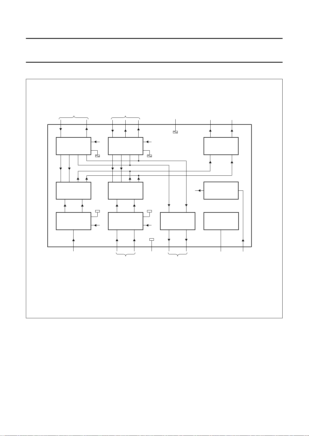
BLOCK DIAGRAM
handbook, full pagewidth
band A oscillator
tuned circuit
BAND A
OSCILLATOR
band C oscillator
tuned circuit
BAND C
OSCILLATOR
MIXERMIXER
111213151416
TDA5630BT
IF outputsGND
IF
AMPLIFIER
ELECTRONIC
BAND SWITCH
TDA5630BT
910
BAND A
STAGE
band A input local oscillator
BAND C
STAGE
band C inputs
3214 76
RF
GND
LOCAL
OSCILLATOR
AMPLIFIER
amplifier outputs
Fig.1 Block diagram.
DC
STABILIZER
5 8
V band switch
P
MBE319
input
1996 Jun 06 3
Philips Semiconductors Product specification
9 V VHF and UHF mixer/oscillator for TV
and VCR cable tuners
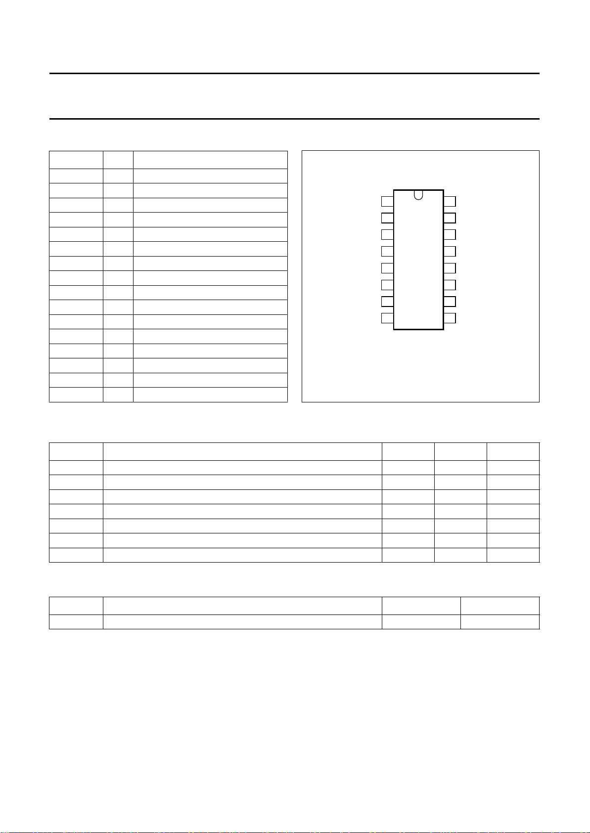
PINNING
SYMBOL PIN DESCRIPTION
CIN1 1 band C input 1
CIN2 2 band C input 2
RFGND 3 ground for RF inputs
AIN 4 band A input
V
P
LOOUT1 6 local oscillator amplifier output 1
LOOUT2 7 local oscillator amplifier output 2
BS 8 band switch input
IFOUT1 9 IF amplifier output 1
IFOUT2 10 IF amplifier output 2
GND 11 ground (0 V)
COSCOC1 12 band C oscillator output collector 1
COSCOC2 13 band C oscillator output collector 2
AOSCOC 14 band A oscillator output collector
COSCIB 15 band C oscillator input base
AOSCIB 16 band A oscillator input base
5 supply voltage
handbook, halfpage
1
2
CIN2
AIN
V
BS
3
4
5
P
6
7
8
TDA5630BT
RFGND
LOOUT1
LOOUT2
Fig.2 Pin configuration.
TDA5630BT
16
AOSCIBCIN1
15
COSCIB
14
AOSCOC
13
COSCOC2
12
COSCOC1
11
GND
10
IFOUT2
9
IFOUT1
MBE318
LIMITING VALUES
In accordance with the Absolute Maximum Rating System (IEC 134).
SYMBOL PARAMETER MIN. MAX. UNIT
V
P
V
SW
I
O
t
s(max)
T
stg
T
amb
T
j
supply voltage −0.3 +10.5 V
switching voltage 0 10.5 V
output current of each pin referenced to ground −−10 mA
maximum short-circuit time (all pins) − 10 s
IC storage temperature −55 +150 °C
operating ambient temperature −10 +70 °C
junction temperature − 150 °C
THERMAL CHARACTERISTICS
SYMBOL PARAMETER VALUE UNIT
R
th j-a
thermal resistance from junction to ambient in free air 115 K/W
HANDLING
Human body model: the IC withstands 2000 V in accordance with the UZW-B0/FQ-A302 specification equivalent to the
MIL-STD-883C category B (2000 V)
(stress reference pins RFGND, GND and V
short-circuited together).
P
Machine model: the IC withstands 200 V in accordance with the UZW-B0/FQ-B302 specification
(issue date: Nov 6th, 1990)
(stress reference pins RFGND, GND and VP short-circuited together).
1996 Jun 06 4
Philips Semiconductors Product specification
9 V VHF and UHF mixer/oscillator for TV
TDA5630BT
and VCR cable tuners
CHARACTERISTICS
V
=9V; T
P
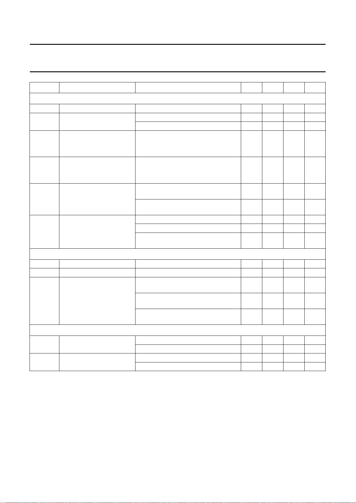
SYMBOL PARAMETER CONDITIONS MIN. TYP. MAX. UNIT
Supply
V
P
I
P
V
SW
I
SW
Band A mixer including IF amplifier
f
RF
f
max
G
v
NF noise figure f
V
o
V
i
g
os
g
i
C
i
Band A oscillator
f
osc
f
shift
f
drift
=25°C; measured in circuit of Fig.11; unless otherwise specified.
amb
supply voltage 8.1 9.0 9.9 V
supply current 35 48 55 mA
switching voltage band A 0 − 1.1 V
band C 3.0 − 5.0 V
switching current band A −−2µA
band C −−10 µA
frequency range note 1; Vt= 0.45 to 28 V 45 − 300 MHz
maximum frequency note 1 − 470 − MHz
voltage gain fRF= 50 MHz; see Fig.3; note 2 22.5 25 27.5 dB
= 300 MHz; see Fig.3; note 2 22.5 25 27.5 dB
f
RF
= 470 MHz; see Fig.3; note 2 − 25 − dB
f
RF
= 50 MHz; see Figs 4 and 5 − 7.5 8.5 dB
RF
= 180 MHz; see Figs 4 and 5 − 910dB
f
RF
= 300 MHz; see Fig.5 − 10.5 11.5 dB
f
RF
output voltage causing 1% cross modulation in channel;
115 118 − dBµV
fRF= 300 MHz; see Fig.6
input voltage causing 10 kHz pulling in channel;
− 104 − dBµV
fRF= 300 MHz; note 3
optimum source
conductance for noise figure
fRF=50MHz − 0.5 − mS
= 180 MHz − 1.1 − mS
f
RF
input conductance fRF= 50 MHz; see Fig.12; note 4 − 0.26 − mS
= 180 MHz; see Fig.12; note 4 − 0.35 − mS
f
RF
input capacitance fRF= 50 to 180 MHz; see Fig.12; note 4 − 2 − pF
frequency range note 5; Vt= 0.45 to 28 V 80 − 336 MHz
frequency shift ∆VP= 10%; note 6 −−200 kHz
frequency drift ∆T=25°C with no compensation;
−−500 kHz
NP0 capacitors; note 7
5 s to 15 min after switch on; with no
− 500 950 kHz
compensation; NP0 capacitors; note 8
5 s to 15 min after switch on; with
− 200 300 kHz
compensation; note 9
1996 Jun 06 5
Philips Semiconductors Product specification
9 V VHF and UHF mixer/oscillator for TV
TDA5630BT
and VCR cable tuners
SYMBOL PARAMETER CONDITIONS MIN. TYP. MAX. UNIT
Band C mixer including IF amplifier; measurements using hybrid; note 10
f
RF
G
v
NF noise figure not corrected for image
V
o
V
i
Z
i
frequency range Vt= 0.45 to 28 V; note 1 430 − 860 MHz
voltage gain fRF= 430 MHz; see Fig.7; note 2 33 36 39 dB
= 860 MHz; see Fig.7; note 2 33 36 39 dB
f
RF
fRF= 430 MHz; see Fig.8 − 910dB
= 860 MHz; see Fig.8 − 11 12 dB
f
RF
output voltage causing 1% cross modulation in channel
f
= 430 MHz; see Fig.9 116 120 − dBµV
RF
= 860 MHz; see Fig.9 116 120 − dBµV
f
RF
input voltage causing 10 kHz pulling in channel;
− 84 − dBµV
fRF= 860 MHz; note 3
causing N + 5 - 1 MHz pulling;
= 820 MHz; see Fig.10
f
RF
− 63 − dBµV
input impedance (RS+jLSω)RS at fRF= 430 MHz; see Fig.13; note 4 − 40 −Ω
at fRF= 860 MHz; see Fig.13; note 4 − 53 −Ω
R
S
at fRF= 430 to 860 MHz; see Fig.13;
L
S
− 9 − nH
note 4
Band C oscillator
f
f
f
osc
shift
drift
frequency range note 5; Vt= 0.45 to 28 V 470 − 900 MHz
frequency shift ∆VP= 10%; note 6 −−400 kHz
frequency drift ∆T=25°C with no compensation;
IF amplifier
s
22
Z
o
output reflection coefficient magnitude; see Fig.14; note 4 −−10 − dB
output impedance
(RS+jLSω)
−−2.5 MHz
NP0 capacitors; note 7
5 s to 15 min after switch on; with no
− 1000 1300 kHz
compensation; NP0 capacitors; note 8
5 s to 15 min after switch on; with
− 550 950 kHz
compensation; note 9
phase; see Fig.14; note 4 − 9 −
o
RS; see Fig.14; note 4 − 95 −Ω
; see Fig.14; note 4 − 45 − nH
L
S
1996 Jun 06 6
 Loading...