

Philips TDA5341 Datasheet

INTEGRATED CIRCUITS
DATA SH EET
TDA5341
Brushless DC motor and VCM drive
circuit with speed control
Product specification
File under Integrated Circuits, IC11
1997 Jul 10

Philips Semiconductors Product specification
Brushless DC motor and VCM drive circuit
with speed control
FEATURES
• Full-wave commutation (using push-pull output stages)
without position sensors
• Built-in start-up circuitry
• Three push-pull MOS outputs:
– 1 A output current
– Low voltage drop
– Built-in current limiter
• Thermal protection
• General purpose operational amplifier
• Reset generator
• Motor brake facility
• Actuator driver (H-bridge current-controlled)
• Power-down detector
• Automatic park and brake procedure
• Adjustable park voltage
• Sleep mode
• Speed control with Frequency-Locked Loop (FLL)
• Serial port
• Friction reduction prior to spin-up.
APPLICATIONS
• Hard Disk Drive (HDD).
GENERAL DESCRIPTION
The TDA5341 is a BiCMOS integrated circuit used to drive
brushless DC motors in full-wave mode. The device
senses the rotor position using an EMF sensing technique
and is ideally suited as a drive circuit for a hard disk drive
motor.
The TDA5341 also includes a Voice Coil Motor driver
(VCM), reset and park facilities and an accurate speed
regulator. In addition, a serial port facilitates the control of
the device.
TDA5341
QUICK REFERENCE DATA
Measured over full voltage and temperature range.
SYMBOL PARAMETER MIN. TYP. MAX. UNIT
V
DD
I
oMOT
R
DS(MOT)
I
oACT
R
DS(ACT)
ORDERING INFORMATION
TYPE
NUMBER
TDA5341G LQFP64
general supply voltage for logic and power 4.5 5.0 5.25 V
motor output current 1.3 1.6 1.9 A
motor output resistance − 1.1 1.56 Ω
actuator output current 0.7 1.1 1.4 A
actuator output resistance − 2.0 2.5 Ω
PACKAGE
NAME DESCRIPTION VERSION
plastic low profile quad flat package; 64 leads; body 10 × 10 × 1.4 mm
SOT314-2
1997 Jul 10 2
Philips Semiconductors Product specification
Brushless DC motor and VCM drive circuit
with speed control
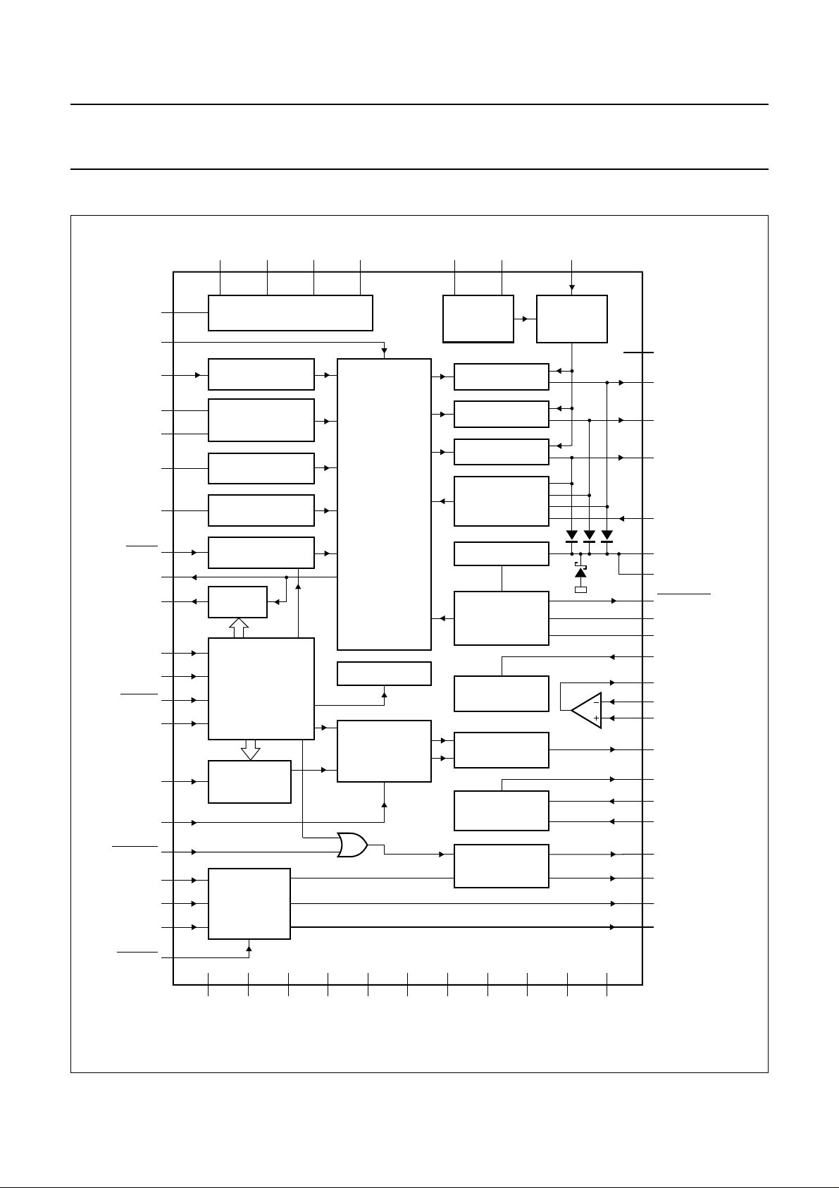
BLOCK DIAGRAM
handbook, full pagewidth
CAPCP
FREDENA
TESTIN
CAPCDM
CAPCDS
CAPTI
CAPST
BRAKE
FG
FMOT
CLOCK
DATA
ENABLE
RESET
ROSC
DPULSE
RETRACT
V
CMIN1
V
CMIN2
V
ref
GAINSEL
CAPXA
27
9
12
18
19
2
1
11
10
58
39
38
42
57
48
35
30
33
34
36
15
CAPXB
UPPER VOLTAGE
THERMAL
SWITCH
ADAPTIVE
COMMUTATION
DELAY
TIMING
OSCILLATOR
START
OSCILLATOR
BRAKE
CONTROLLER
POLES
DIVIDER
SERIAL
PORT
PROGRAMMING
FREQUENCY
DIVIDER
VCM
PREAMPLIFIER
50 14 55 31 49 17
CAPYA
CONVERTER
CAPYB
COMMUTATION
AND
OUTPUT
DRIVING
LOGIC
brake
BAND GAP 1
sleep
fill
DIGITAL
FREQUENCY
COMPARATOR
park
CNTRL
CAPCPC
222463625961
CONTROL
AMPLIFIER
POWER 1
POWER 2
POWER 3
COMPARATORS
BAND GAP 2
UNDER-VOLTAGE
DETECTOR
BRAKE
AFTER PARK
CHARGE
PUMP
SENSE
AMPLIFIER
VCM
H-BRIDGE
CURRENT
LIMIT
CONTROL
TDA5341
25 64 40 16 41
ILIM
TDA5341
23
20
PRESET
60
MOT1
8
MOT2
21
MOT3
7
MOT0
3
CLAMP1
26
CLAMP2
43
RESETOUT
44
UVDIN1
54
UVDIN2
46
BRAKEDELAY
4
AMPOUT
5
AMPIN−
6
AMPIN+
32
FILTER
53
SENSEOUT
52
SENSEIN+
51
SENSEIN−
37
VCM+
45
VCM−
28
FB1
29
FB2
V
EEDVEE1VEE2VEE3VEE4VEEVDD1VDD2VDD3VDDVDDD
Fig.1 Block diagram.
1997 Jul 10 3
MGE817

Philips Semiconductors Product specification
Brushless DC motor and VCM drive circuit
TDA5341
with speed control
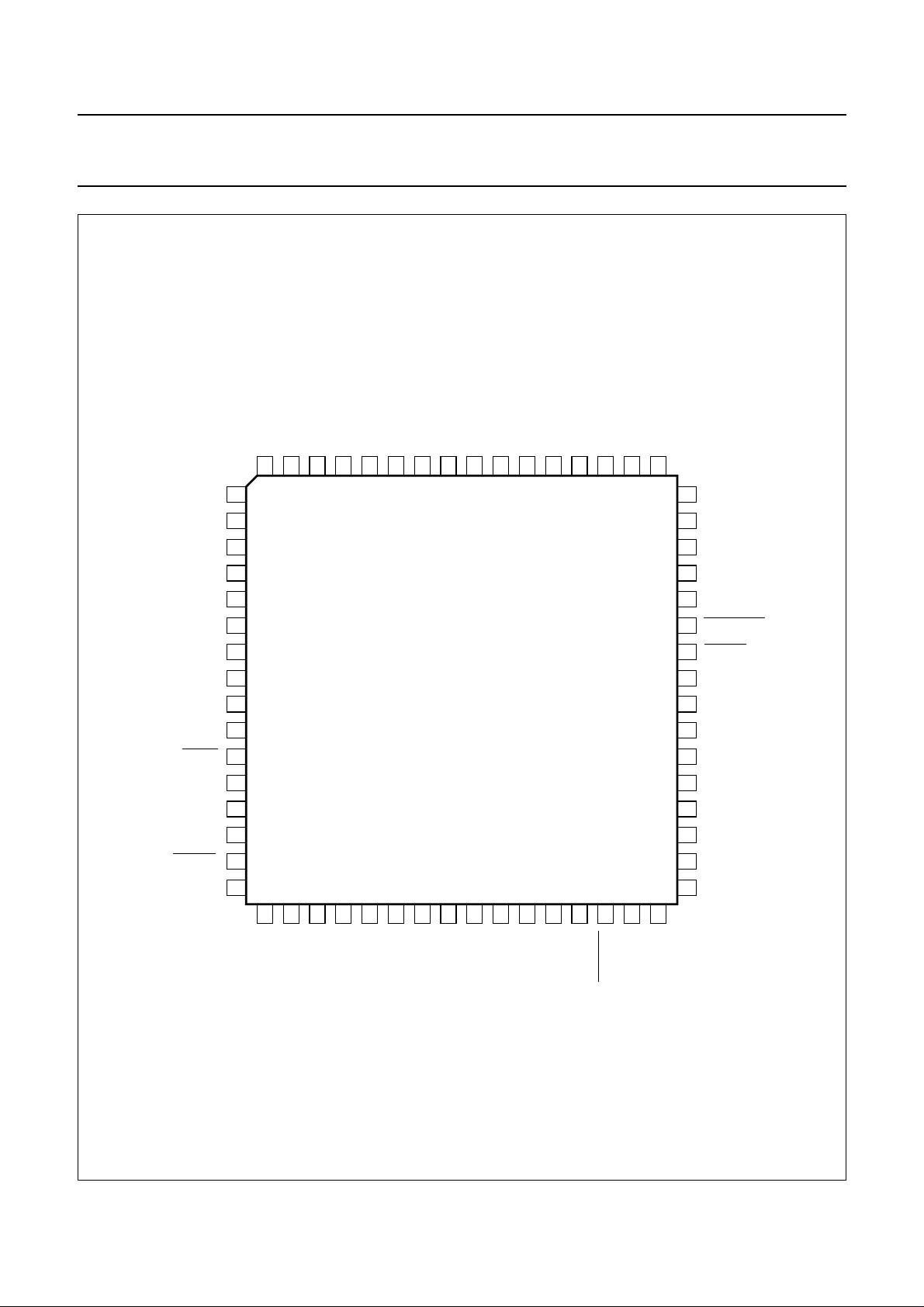
PINNING
SYMBOL PIN DESCRIPTION
CAPST 1 external capacitor for starting oscillator
CAPTI 2 external capacitor for timer circuit
CLAMP1 3 external capacitor used to park the heads; must be externally connected to CLAMP2
AMPOUT 4 uncommitted operational amplifier output
AMPIN− 5 uncommitted operational amplifier invert input
AMPIN+ 6 uncommitted operational amplifier direct input
MOT0 7 motor centre tap input
MOT2 8 motor driver output 2
FREDENA 9 friction reduction mode enable input (active HIGH)
FG 10 frequency generator (tacho) output
BRAKE 11 brake input command (active LOW)
TESTIN 12 test input for power output switch-off (active HIGH)
TP1 13 test purpose 1 (should be left open-circuit)
V
EE1
GAINSEL 15 VCM gain adjustment input (switch ON when GAINSEL is LOW)
V
DD
V
EE
CAPCDM 18 external capacitor for adaptive commutation delay (master)
CAPCDS 19 external capacitor for adaptive commutation delay (slave)
PRESET 20 set the motor drivers into a fixed state: MOT1 = F (floating), MOT2 = L, MOT3 = H
MOT3 21 motor driver output 3
CAPCPC 22 frequency compensation of the current control
ILIM 23 current limit control input
CNTRL 24 motor control
V
DD1
CLAMP2 26 external capacitor used to park the heads; must be externally connected to CLAMP1
CAPCP 27 external capacitor for the charge pump output
FB1 28 output of the VCM preamplifiers
FB2 29 switchable output of the VCM preamplifier
RETRACT 30 park input command (active LOW)
V
EE3
FILTER 32 charge pump output to be connected to an external filter
V
CMIN1
V
CMIN2
DPULSE 35 data pulse input of the frequency comparator of the speed control
V
ref
VCM+ 37 positive output of the VCM amplifier
DATA 38 input data of the serial port (active HIGH)
CLOCK 39 clock input signal to shift DATA into SERIALIN register (active HIGH)
V
DD3
14 ground for the spindle motor drivers
16 general power supply
17 general ground
25 power supply 1 for the spindle motor drivers
31 ground 3 for the actuator driver
33 VCM voltage control input
34 switchable VCM voltage control input
36 voltage reference input
40 power supply 3 for the actuator driver
1997 Jul 10 4

Philips Semiconductors Product specification
Brushless DC motor and VCM drive circuit
TDA5341
with speed control
SYMBOL PIN DESCRIPTION
V
DDD
ENABLE 42 enable input; enables the serial port, i.e. allows DATA to be shifted in (active LOW)
RESETOUT 43 under-voltage detector output flag (active LOW)
UVDIN1 44 external capacitor for the
VCM− 45 negative output of the VCM amplifier
BRAKEDELAY 46 delay control input for brake after park
TP2 47 test purpose 2 (should be left open-circuit)
ROSC 48 reference oscillator input for motor speed control
V
EE4
V
EED
SENSEIN− 51 inverting input of the VCM sense amplifier
SENSEN+ 52 non-inverting input of the VCM sense amplifier
SENSEOUT 53 output of the VCM sense amplifier
UVDIN2 54 external voltage reference for the under-voltage detector
V
EE2
TP3 56 test purpose 3 (should be left open-circuit)
RESET 57 reset input; forces all bits of the SERIALIN register to 0 (active HIGH)
FMOT 58 tachometer output (one pulse per mechanical revolution)
CAPXB 59 external capacitor for the charge pump output
MOT1 60 motor driver output 1
CAPXA 61 external capacitor for the charge pump output
CAPYA 62 external capacitor for the charge pump output
CAPYB 63 external capacitor for the charge pump output
V
DD2
41 digital power supply
RESETOUT duration
49 ground 4 for the actuator driver
50 digital ground
55 ground 2 for the spindle motor drivers
64 power supply for the spindle motor drivers
1997 Jul 10 5
Philips Semiconductors Product specification
Brushless DC motor and VCM drive circuit
with speed control
handbook, full pagewidth
DD2
CAPYB
CAPST
CAPTI
CLAMP1
AMPOUT
AMPIN−
AMPIN+
MOT0
MOT2
FREDENA
FG
BRAKE
TESTIN
TP1
V
EE1
GAINSEL
V
DD
V
64
1
2
3
4
5
6
7
8
9
10
11
12
13
14
15
16
17
EE
V
CAPYA
63
62
18
19
CAPCDS
CAPCDM
CAPXA
MOT1
61
60
20
21
MOT3
PRESET
FMOT
CAPXB
59
58
TDA5341
22
23
ILIM
CAPCPC
RESET
57
24
CNTRL
TP3
56
25
DD1
V
EE2
V
UVDIN2
55
54
26
27
CAPCP
CLAMP2
SENSEIN+
SENSEOUT
53
52
28
29
FB2
FB1
EED
SENSEIN−
V
51
50
30
31
EE3
V
RETRACT
EE4
V
49
48
47
46
45
44
43
42
41
40
39
38
37
36
35
34
33
32
FILTER
TDA5341
ROSC
TP2
BRAKEDELAY
VCM−
UVDIN1
RESETOUT
ENABLE
V
DDD
V
DD3
CLOCK
DATA
VCM+
V
ref
DPULSE
V
CMIN2
V
CMIN1
MGE816
Fig.2 Pinning diagram.
1997 Jul 10 6

Philips Semiconductors Product specification
Brushless DC motor and VCM drive circuit
with speed control
FUNCTIONAL DESCRIPTION
The TDA5341 offers a sensorless three-phase motor
full-wave drive function. The device also offers protected
outputs capable of handling high currents and can be used
with star or delta connected motors.
The TDA5341 can easily be adapted for different motors
and applications.
The TDA5341 offers the following features:
• Sensorless commutation by using the motor EMF
• Built-in start-up circuit
• Optimum commutation, independent of motor type or
motor loading
• Built-in flyback diodes
• Three-phase full-wave drive
• High output current (1.3 A)
• Low MOS R
• Outputs protected by current limitation and thermal
protection of each output transistor
• Low current consumption
• Additional uncommitted operational amplifier
• H-bridge actuator driver current controlled with an
external series sense resistor
• Automatic retract procedure
• Adjustable park voltage
• Sleep mode
• Automatic brake (after park) procedure
DSon
(1 Ω)
TDA5341
• Speed control based on FLL technique
• Serial port DATAIN (24 bits)
• Friction reduction prior to spin-up.
TDA5341 modes description
The TDA5341 can be used in two main modes, depending
on whether they are controlled or not.
The ‘controlled modes’ (user commands) are executed by
the TDA5341 without delay or priority treatment, either by
software via the serial port or by hardware. BRAKE is a
hardware command whereas RETRACT can be controlled
in both ways. If it is preferable to control the heads parking
via the serial bus, the equivalent pin can be left
open-circuit.
The sleep mode is controlled by software only; it results
from the combination of the spindle and actuator being
disabled. The spindle is turned off by bit SPINDLE
DISABLE, whereas the actuator is disabled towards bit
VCM DISABLE of the serial port (see Section “Serial
port”). In addition, a special spin-up mode can be activated
in the event of high head stiction
The ‘uncontrolled modes’ only result from different failures
caused by either a too high internal temperature or an
abnormally low power voltage, which will cause the
actuator to retract and, after the spindle, to brake.
The output signals mainly affected by those failures are
RESETOUT, MOT1, 2 and 3, VCM+ and VCM−. This is
summarised in Tables 1 and 2.
Table 1 Summary of controlled modes
HARDWARE/
SOFTWARE
Software spindle disable high impedance high impedance HIGH spindle off
Software VCM disable not affected high impedance HIGH spindle on; VCM off
Hardware brake LOW not affected HIGH spindle coils ground
Software/
hardware
Hardware friction reduction − not affected HIGH heads in vibration
1997 Jul 10 7
MODE MOT1, 2 AND 3
retract not affected VCM− = 0.65 V;
VCM+ AND
VCM−
VCM+=0V
RESETOUT EFFECT
HIGH heads parked

Philips Semiconductors Product specification
Brushless DC motor and VCM drive circuit
with speed control
Table 2 Summary of uncontrolled modes
FAILURE MOT1, 2 AND 3 VCM+ AND VCM− RESETOUT EFFECT
Thermal
shut-down
Voltage
shut-down
Controlled modes
S
PINDLE DISABLE
The spindle circuitry is switched off when bit 23 (SPINDLE
DISABLE) of the serial port is pulled HIGH. In that mode,
the reference band gap generator is cut off so that all
internal current sources are disabled. Both the spindle and
actuator outputs will be set to the high impedance state
because the upper converter is also turned off.
It should be noted that the uncommitted operational
amplifier is also disabled in that mode.
VCM
DISABLE
The actuator will be disabled when bit 22 (VCM DISABLE)
is set to logic 1; the spindle circuitry is not affected in that
mode. The retract circuitry also remains active, so that the
heads can be parked although the VCM is disabled. In that
mode, the current consumption can be reduced by ±4 mA.
high impedance → LOW VCM− = 0.65 V;
VCM+ = 0 V
high impedance → LOW VCM− = 0.65 V;
VCM+ = 0 V
RICTION REDUCTION
F
Pulling FREDENA HIGH activates the friction reduction
mode of the TDA5341. In that mode, a clock signal fed via
pin TESTIN will cause the MOT outputs to sequentially
switch-on and switch-off at the same frequency and, as a
result, generate an AC spindle torque high enough to
overcome the head stiction.
Before start-up, the head stiction might be higher than
normal due to condensation between the head(s) and the
disk(s). Normal spin-up is not possible when this friction
torque is higher than the start-up torque of the spindle
motor. Spin-up is then only possible after friction has been
reduced by breaking the head(s) free. Bringing a static
friction system into mechanical resonance is an effective
method to break static friction head(s) free.
The resonance frequency is:
f
res
1
×=
------ -
2π
LOW automatic park and brake
LOW automatic park and brake
C
0.5
--- -
J
TDA5341
S
LEEP MODE
The sleep mode is obtained by pulling both the SPINDLE
and VCM DISABLE bits of the serial port HIGH. The power
monitor circuitry only remains active in sleep mode.
ETRACT
R
Retract is activated by pulling either bit 21 (PARK) HIGH
or RETRACT (pin 30) LOW. WhenRETRACT is set LOW,
a voltage of 0.65 V is applied to pin VCM− for parking.
It should be noted that the park voltage can be made
adjustable by changing one of the interconnect masks.
Accordingly, some different voltages, varying from
0.2 to 1.2 V, can quickly be obtained on customer
demand. This mode does not affect the control of the
spindle rotation.
B
RAKE MODE
The brake mode is activated by pulling BRAKE (pin 11)
LOW. When a voltage of less than 0.8 V is applied to pin
BRAKE, the 3 motor outputs are short-circuited to ground,
which results in a quick reduction of the speed until the
motor stops completely.
Where:
C = Stiffness of the head-spring(s) in direction of disk(s)
rotation, (N/m)
2
J = Inertia of the disk(s), (kg/m
).
The external clock input frequency must be:
f
clk
6
------ -
2π
C
0.5
×=
--- -
J
A burst of n × 6 clock pulse will bring the system into
resonance and break the heads free (n > 2). Once the
heads have been broken free, the normal spin-up
procedure can be applied.
It should be noted that the clock frequency must be smaller
than 40000/CAPCDM (nF).
1997 Jul 10 8

Philips Semiconductors Product specification
Brushless DC motor and VCM drive circuit
with speed control
Uncontrolled modes
P
OWER SHUT-DOWN
If the power supply decreases to less than the voltage
threshold determined by the ratio between R1 and R2
connected to UVDIN2 (see Fig.8) (for more than 1 µs), the
TDA5341 will issue a reset (RESETOUT goes LOW) and
the following operation will start:
• Firstly, the MOT outputs are switched to the high
impedance state so as to get back the rectified EMF
issued from the motor itself. At the same time, the
voltage upper converter is cut off in order to preserve the
voltage on the charge pump capacitance at CAPCP.
The energy supplied in that way is then used to park the
heads in a safe position
• Secondly, after a certain period of time, depending on
the RC constant of the device connected to
BRAKEDELAY, the lower MOS drivers will be turned on
in order to stop the motor completely.
TDA5341
The system will only function when the EMF voltage from
the motor is present. Consequently, a start oscillator is
provided that will generate commutation pulses when no
zero-crossings in the motor voltage are available.
A timing function is incorporated into the device for internal
timing and for timing of the reverse rotation detection.
The TDA5341 also contains a control amplifier, directly
driving output amplifiers.
The TDA5341 also provides access to the user of some of
its internal test modes. Firstly, a PRESET mode can be
used for prepositioning the three motor output drivers into
a fixed state. By pulling pin PRESET to 0.75 V above V
MOT3 goes HIGH, MOT2 goes LOW and MOT1 goes to
the high impedance state.
In addition, when TESTIN is pulled HIGH (provided that
FREDENA is LOW), the 3 motor output drivers are
switched off. It should be noted that RESETOUT goes
LOW in that particular event.
DD
,
T
HERMAL SHUT-DOWN
Should the temperature of the chip exceed +140 ±10 °C, a
shut-down operation will also be processed. The actions
described for power shut-down will be sequenced in the
same manner.
PINDLE SECTION (see Fig.1)
S
Full-wave driving of a three-phase motor requires three
push-pull output stages. In each of the six possible states
two outputs are active, one sourcing current and one
sinking current. The third output presents a high
impedance to the motor which enables measurement of
the motor EMF in the corresponding motor coil by the EMF
comparator at each output. The commutation logic is
responsible for control of the output transistors and
selection of the correct EMF comparator.
The zero-crossing in the motor EMF (detected by the
comparator selected by the commutation logic) is used to
calculate the correct moment for the next commutation, i.e.
the change to the next output state. The delay is calculated
(depending on the motor loading) by the adaptive
commutation delay block.
Because of high inductive loading the output stages
contain flyback diodes. The output stages are also
protected by a current limiting circuit and by thermal
protection of the six output transistors.
The zero-crossings can be used to provide speed
information such as the tacho signal (FG).
Adjustments
The system has been designed in such a way that the
tolerances of the application components are not critical.
However, the approximate values of the following
components must still be determined:
• The start capacitor; this determines the frequency of the
start oscillator
• The two capacitors in the adaptive commutation delay
circuit; these are important in determining the optimum
moment for commutation, depending on the type and
loading of the motor
• The timing capacitor; this provides the system with its
timing signals.
The start capacitor (CAPST)
This capacitor determines the frequency of the start
oscillator. It is charged and discharged, with a current of
5.5 µA, from 0.05 to 2.2 V and back to 0.05 V. The time
taken to complete one cycle is given by:
t
= (0.78 × C); where C is given in µF.
start
The start oscillator is reset by a commutation pulse and so
is only active when the system is in the start-up mode.
A pulse from the start oscillator will cause the outputs to
change to the next state (torque in the motor). If the
movement of the motor generates enough EMF the
TDA5341 will run the motor.
1997 Jul 10 9
 Loading...