Philips TDA5333T-C5, TDA5332T-C5 Datasheet

DATA SH EET
Preliminary specification
File under Integrated Circuits, IC02
March 1989
INTEGRATED CIRCUITS
TDA5332T
Double mixer/oscillator for TV and
VCR tuners

March 1989 2
Philips Semiconductors Preliminary specification
Double mixer/oscillator for TV and VCR
tuners
TDA5332T
GENERAL DESCRIPTION
The TDA5332T is an integrated circuit that performs the mixer/oscillator functions in TV and VCR tuners. This device
gives the designer the capability to design an economical and physically small tuner which will be capable of meeting the
most stringent requirements e.g. FTZ or FCC. The tuner development time can be drastically reduced by using this
device.
Features
• Balanced mixer with a common emitter input for band A
• Amplitude-controlled oscillator for band A
• Balanced mixer with common base input for band B
• Balanced oscillator for band B
• SAW filter preamplifier with an output impedance of 75 Ω in application
• Bandgap voltage stabilizer for oscillator stability
• Electronic bandswitch
QUICK REFERENCE DATA
PACKAGE OUTLINE
20-lead mini-pack, plastic (SO20L; SOT163A); SOT163-1; 1996 November 29.
PARAMETER CONDITIONS SYMBOL MIN. TYP. MAX. UNIT
Supply voltage V
P
− 12 − V
Band A frequency range depending on application f
A
45 − 470 MHz
Band B frequency range depending on application f
B
160 − 860 MHz
Band A noise factor 50 MHz NF
A
− 7.5 − dB
Band B noise factor 860 MHz NF
B
− 9 − dB
Band A input voltage 1% cross-modulation V
18-20
− 100 − dBµV
Band B input power 1% cross-modulation
note 5 P
I
−−21 − dBm
Band A voltage gain G
VA
− 25 − dB
Band B voltage gain G
VB
− 36 − dB

March 1989 3
Philips Semiconductors Preliminary specification
Double mixer/oscillator for TV and VCR
tuners
TDA5332T
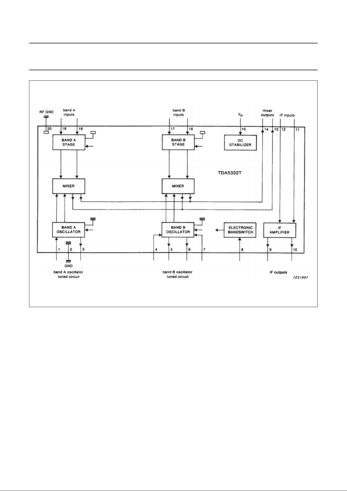
Fig.1 Block diagram.

March 1989 4
Philips Semiconductors Preliminary specification
Double mixer/oscillator for TV and VCR
tuners
TDA5332T
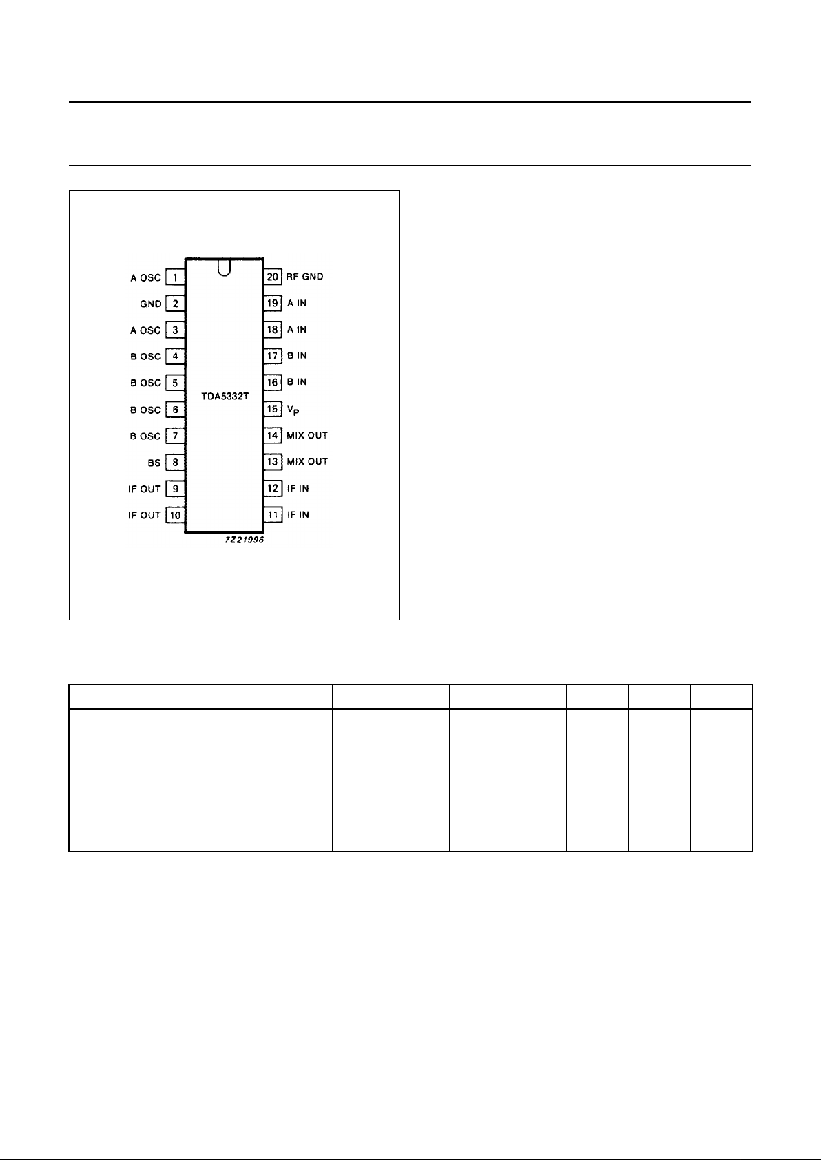
Fig.2 Pinning diagram.
PINNING
1 A OSC band A oscillator input
2 GND ground (0 V)
3 A OSC band A oscillator output
4 B OSC band B oscillator input
5 B OSC band B oscillator output
6 B OSC band B oscillator output
7 B OSC band B oscillator input
8 BS electronic bandswitch
9 IF OUT IF amplifier output
10 IF OUT IF amplifier output
11 IF IN IF amplifier input
12 IF IN IF amplifier input
13 MIX OUT mixer output
14 MIX OUT mixer output
15 V
P
positive supply voltage
16 B IN band B input
17 B IN band B input
18 A IN band A input
19 A IN band A input
20 RF GND ground for RF inputs
RATINGS
Limiting values in accordance with the Absolute Maximum System (IEC 134)
THERMAL RESISTANCE
HANDLING
Pins 8, 9 and 10 withstand the ESD test in accordance with MIL-STD-883C category B (2000 V).
PARAMETER CONDITIONS SYMBOL MIN. MAX. UNIT
Supply voltage V
P
−0.3 14 V
Switching voltage V
8
014V
Output current of each pin to ground I
O
−−10 mA
Maximum short-circuit time (all pins) t
SC
− 10 s
Storage temperature range T
stg
−55 + 150 °C
Operating ambient temperature range T
amb
−25 + 80 °C
Junction temperature T
j
−+150 °C
From junction to ambient in free air R
th j-a
typ. 100 K/W
 Loading...