Philips TDA5330T Datasheet

INTEGRATED CIRCUITS
DATA SH EET
TDA5330T
VHF, UHF and Hyperband
mixer/oscillator for TV and VCR
3-band tuners
Product specification
File under Integrated Circuits, IC02
January 1988

Philips Semiconductors Product specification
VHF, UHF and Hyperband mixer/oscillator for
TDA5330T
TV and VCR 3-band tuners
GENERAL DESCRIPTION
The TDA5330T is a monolithic integrated circuit that performs the band A, band B and band C mixer/oscillator functions
in TV and VCR tuners. This device gives the designer the capability to design an economical and physically small 3-band
tuner which will be capable of meeting the most stringent requirements e.g. FTZ or FCC. The tuner development time
can be drastically reduced by using this device.
Features
• Balanced mixer with a common emitter input for band A
• Amplitude-controlled oscillator for band A
• Balanced mixer with common base input for band B and C
• Balanced oscillator for band B and C
• Local oscillator buffer output for external prescaler
• SAW filter preamplifier with an output impedance of 100 Ω
• Bandgap voltage stabilizer for oscillator stability
• Electronic bandswitch
QUICK REFERENCE DATA
PARAMETER CONDITIONS SYMBOL MIN. TYP. MAX. UNIT
Supply voltage V
Band A frequency range f
Band B frequency range f
Band C frequency range f
19−2, 26
A
B
C
− 12 − V
48 − 180 MHz
160 − 470 MHz
430 − 860 MHz
Conversion noise F 7 − 11 dB
Band A input voltage 1% cross-modulation V
Band B and C input power 1% cross-modulation P
Band A voltage gain G
Band B voltage gain G
Band C voltage gain G
24−26
I
v
v
v
− 100 − dBµV
−−21 − dBm
− 24 − dB
− 37 − dB
− 36 − dB
PACKAGE OUTLINE
28-lead mini-pack , plastic (SO20; SOT163A); SOT 163-1; 1996 November 28.
January 1988 2

Philips Semiconductors Product specification
VHF, UHF and Hyperband mixer/oscillator
for TV and VCR 3-band tuners
TDA5330T
January 1988 3
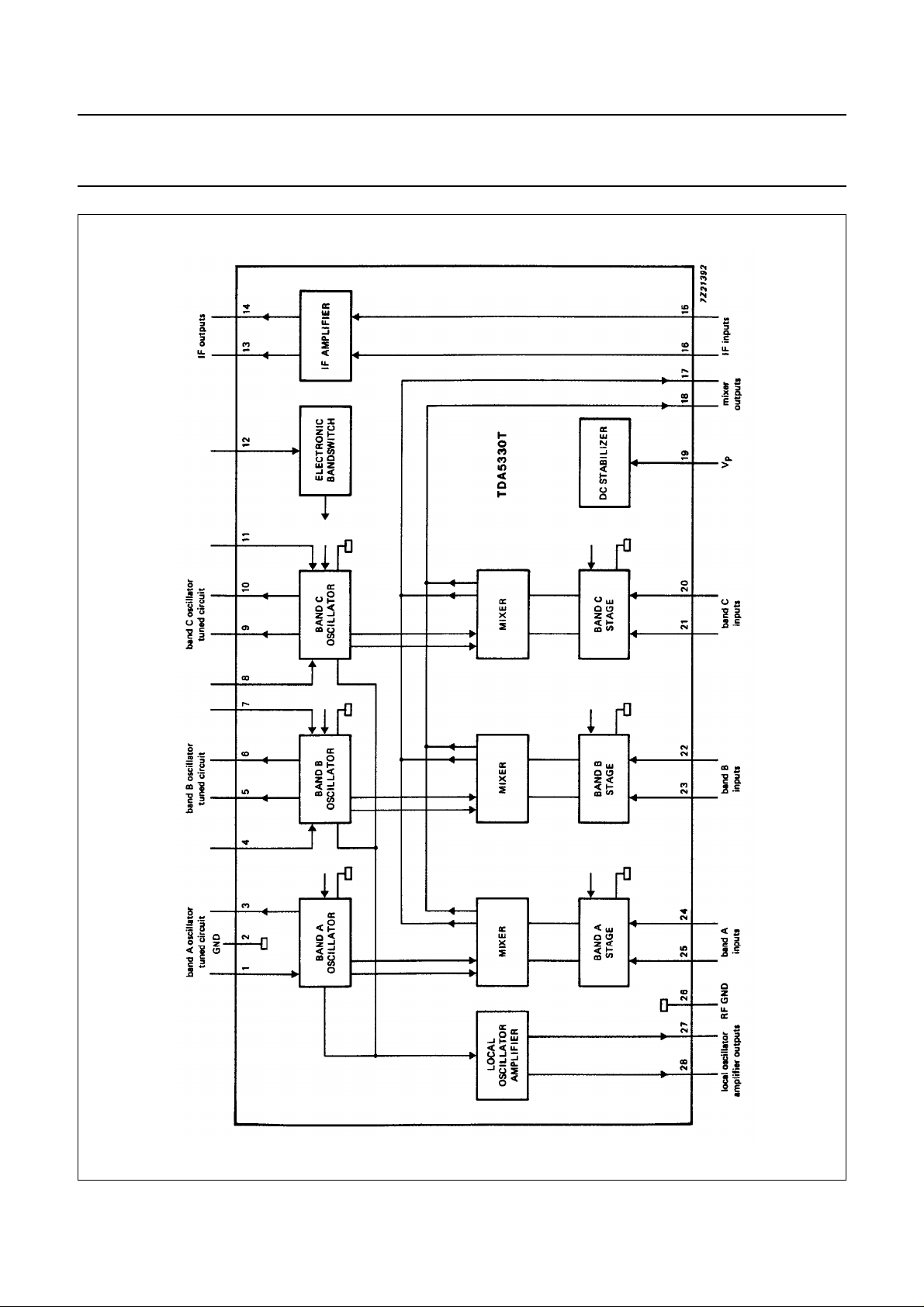
Fig.1 Block diagram.

Philips Semiconductors Product specification
VHF, UHF and Hyperband mixer/oscillator
for TV and VCR 3-band tuners
PINNING
1 A OSC band A oscillator input
2 GND ground (0 V)
3 A OSC band A oscillator output
4 B OSC band B oscillator input
5 B OSC band B oscillator output
6 B OSC band B oscillator output
7 B OSC band B oscillator input
8 C OSC band C oscillator input
9 C OSC band C oscillator output
10 C OSC band C oscillator output
11 C OSC band C oscillator input
12 BS electronic bandswitch
13 IF OUT IF amplifier output
14 IF OUT IF amplifier output
15 IF IN IF amplifier input
16 IF IN IF amplifier input
17 MIX OUT mixer output
18 MIX OUT mixer output
19 V
20 C IN band C input
21 C IN band C input
22 B IN band B input
23 B IN band B input
24 A IN band A input
25 A IN band A input
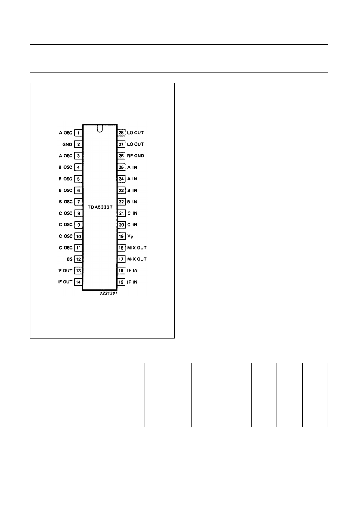
Fig.2 Pinning diagram.
26 RF GND ground for RF inputs
27 LO OUT local oscillator amplifier output
28 LO OUT local oscillator amplifier output
TDA5330T
P
positive supply voltage
RATINGS
Limiting values in accordance with the Absolute Maximum System (IEC 134)
PARAMETER CONDITIONS SYMBOL MIN. MAX. UNIT
Supply voltage V
Switching voltage V
Output current of each pin to ground I
Maximum short-circuit time (all pins) t
Storage temperature range T
Operating ambient temperature range T
P=V19−2, 26
12
O
SC
stg
amb
THERMAL RESISTANCE
From junction to ambient in free air R
th j-a
January 1988 4
−0.3 14 V
014V
−−10 mA
− 10 s
−55 +150 °C
−25 +80 °C
typ. 75 K/W

Philips Semiconductors Product specification
VHF, UHF and Hyperband mixer/oscillator
TDA5330T
for TV and VCR 3-band tuners
CHARACTERISTICS
= 12 V; T
V
P
PARAMETER CONDITIONS SYMBOL MIN. TYP. MAX. UNIT
Supply voltage V
Supply current I
Switching voltage;
band A V
band B V
band C V
Switching current;
band C I
Band A Mixer
(including IF amplifier)
Frequency range f
Noise figure note 1;
Optimum source
conductance 50 MHz G
Input admittance see Fig.9
Input capacitance 50 - 180 MHz C
Input voltage 1% cross-modulation;
Input voltage 10 kHz pulling;
Voltage gain 20 log
Band A mixer
Conversion
transadmittance Sc = I
mixer = −I18/V
Mixer output
admittance pins 15 and 16 − 0.1 − mS
Mixer output
capacitance C
=25°C; unless otherwise specified.
amb
measured using
circuit shown in
Fig.9
50 MHz NF − 7.5 9 dB
180 MHz NF − 910dB
180 MHz G
in channel V
in channel V
(V
13−14/V24
)G
17/V24
24
19−2, 26
19
12
12
12
12
A
24−26
24−26
24−26
24−26
24−26
v
Sc
24−17, 18
17−18
10 − 13.2 V
− 42 55 mA
0 − 1.1 V
1.6 − 2.4 V
3.0 − 5.0 V
−−50 µA
48 − 180 MHz
− 0.5 − mS
− 1.1 − mS
− 2 − pF
97 100 − dBµV
100 108 − dBµV
22.5 25.0 27.5 dB
− 3.5 − mS
− 2 − pF
January 1988 5
 Loading...