

Philips TDA5241 Datasheet
[Q)~u~
~[}{]~~¥
.
Product specification
File under Integrated Circuits, ICO1
Philips
Semiconductors
November 96
re
Philips Semiconductors
Product specification
Brushless DC motor drive circuit
FEATURES
.Full-wave commutation (using push/pull drivers at the output stages) without position sensors
.Built-in start-up circuit
.Optimum commutation independent on motor type or motor loading
.Built-in flyback diodes
.Three push-pull outputs:
-0.85 A output current
-built-in current limiter
.Thermal protection
.Low current consumption by adaptative base-drive
.Tacho output without extra sensor.
..Comparator for external position generator (PG) signal
.Built-in multiplexer combining internal FG and external PG signal on one pin for easy use with a controlling
microprocessor
.Linear control of the output stages
.PG signal output.
TDA5241
APPLICATIONS
.General purpose spindle driver ( e.g. VCR scanner motor).
GENERAL DESCRIPTION
The TDA5241 is a bipolar integrated circuit used to drive brush less DC motors in full-wave mode. The device senses the
rotor position using an EMF-sensing technique and is ideally suited as a drive circuit for VCR scanner motors.
QUICK REFERENCE DATA
~ Measured over full voltage and temperature ranges
SYMBOL
Yp
IUM
Yo
Note
1. An unstabilized supply can be used; Transients of 2 V allowed with max slope 0.1 V/J.ls.
supply voltage range (note 1 } 4
I cu!rent limiting
I oU~Ut voltage at 10 = 100 mA(Upper+Lower transistor)
PARAMETER MIN. TYP.
0.6
0.85
0.93
MAX.
~
~
UNIT
v
A
V
2/19
Philips Semiconductors
Product specification
Brushless DC motor drive circuit
ORDERING INFORMATION
.
TDA5241
.
March 1997
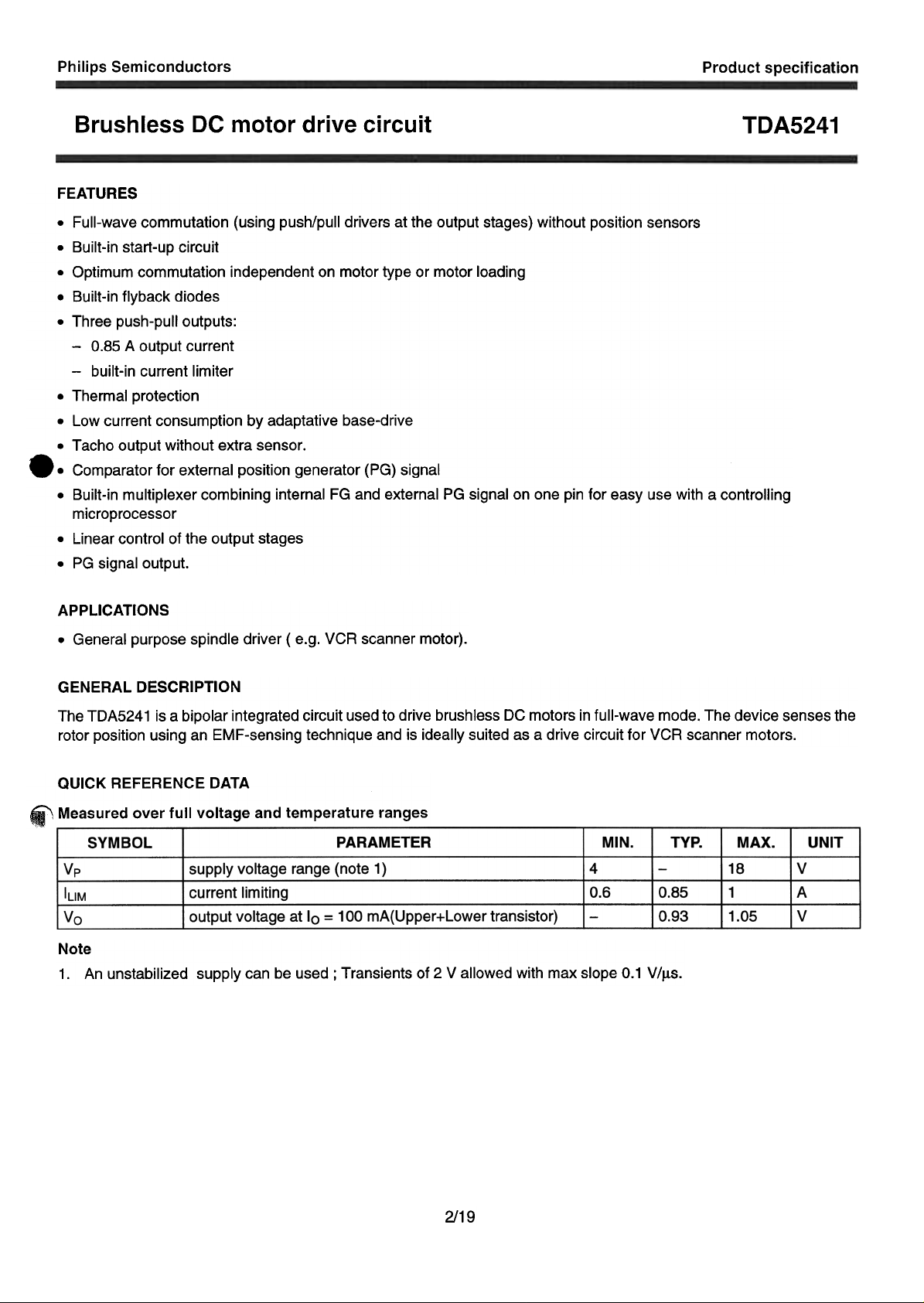
Fig.1 Power derating curve .
3/19
Philips Semiconductors
8
Brushless DC motor drive circuit
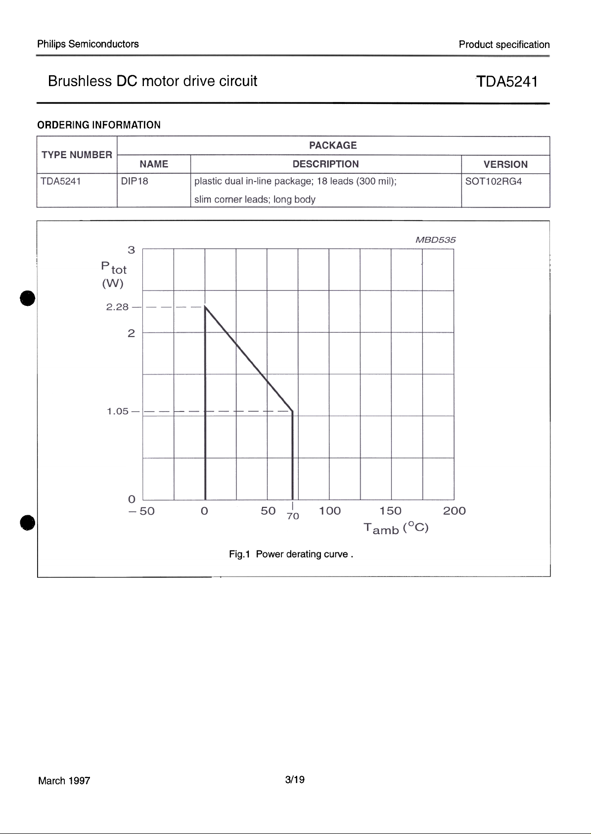
BLOCK DIAGRAM
Product specification
TDA5241
March 1997
4/19
Philips Semiconductors
Product specification
Brushless DC motor drive circuit
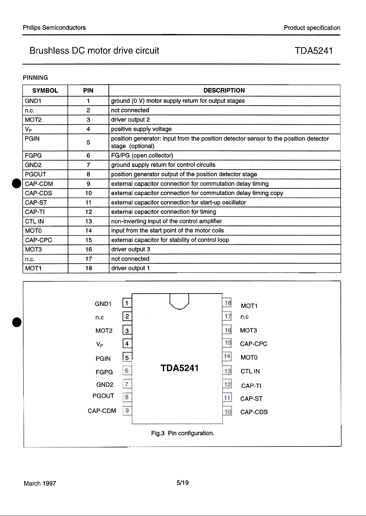
PINNING
SYMBOL PIN
8
GND1
n.c.
MOT2
Vp
PGIN
FGPG
GND2
PGOUT
CAP-CDM
CAP-CDS
CAP-ST
CAP- TI
CTLIN
MOTO
CAP-CPC
MOT3
n.c.
MOT1
1
2
3
4
5
6
7
8
9
10
11
12
13
14
15
16
17
18
ground (0 V) motor supply return for output stages
not connected
driver output 2
Dositive suDDlv voltage
position generator: input from the position detector sensor to the position detector
stage (optional)
FG/PG (open collector)
ground supply return for control circuits
position generator output of the position detector stage
external capacitor connection for commutation delay timing
external capacitor connection for commutation delay timing copy
external capacitor connection for start-up oscillator
external capacitor connection for timing
non-inverting input of the control amplifier
input from the start point of the motor coils
external capacitor for stability of control loop
driver output 3
I not connected
I driver output 1
TDA5241
DESCRIPTION
GND1
n.c
.
u
MOT2
Vp
PGIN
FGPG
GND2
PGOUT
CAP-CDM
10 I
6
7
18
19
TDA5241
18
MOT1
17 n.c
16 MOT3
15
CAP-CPC
14
MOTO
CTLIN
13
12
CAP- TI
CAP-ST
111
CAP-CDS
110
Fig.3 Pin configuration.
March 1997
5/19
Philips Semiconductors
Product specification
Brushless DC motor drive circuit
TDA5241
FUNCTIONAL DESCRIPTION
The TDA5241 offers a sensorless three phase motor drive function. It is unique in its combination of sensorless motor
drive and full-wave drive.
The TDA5241 offers protected outputs capable of handling high currents and can be used with star or delta connected
motors. It can easily be adapted for different motors and applications.
The TDA5241 offers the following features:
.Sensorless commutation by using the motor EMF
.Built-in start-up circuit
.Optimum commutation, independent of motor type or motor loading
.Built-in flyback diodes
.Three phase full-wave drive
..High output current (0.85 A)
.Outputs protected by current limiting and thermal protection of each output transistor
.Low current consumption by adaptive base-drive
.Accurate frequency generator (FG) by using the motor EMF
.Comparator for external position generator (PG) signal
.Built-in multiplexer combining internal FG and external PG signals on one pin for easy use with a controlling
microprocessor
.Linear control of the output stages.
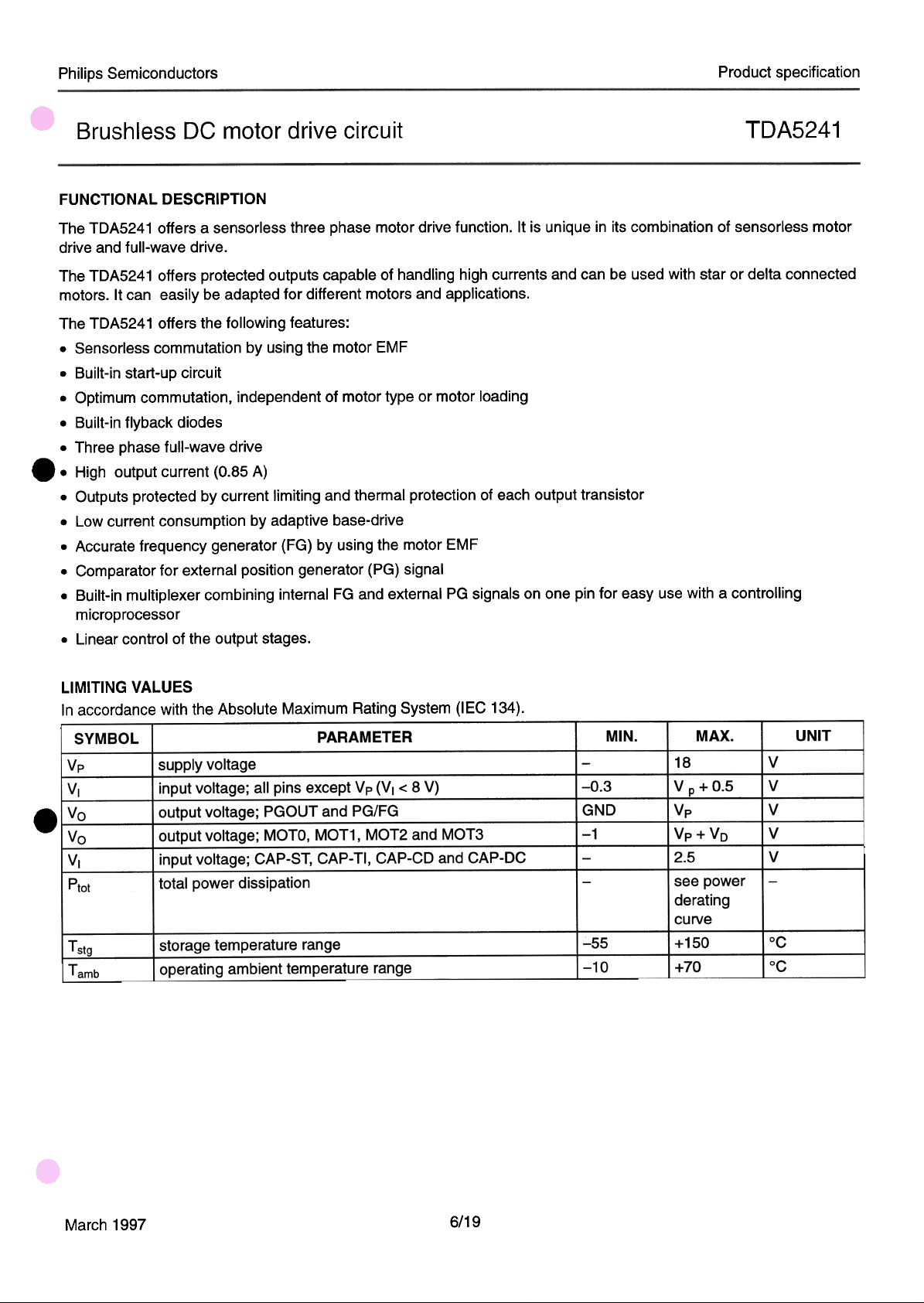
LIMITING VALUES
In accordance with the Absolute Maximum Rating System (IEC 134).
PARAMETER
8
SYMBOL
Vp
VI
1 0
Vo
VI
Ptot
~
Tamb
supply voltage
input voltage; all pins except Vp (VI < 8 V)
output voltage; PGOUT and PG/FG
output voltage; MOTO, MOT1, MOT2 and MOT3
input voltage; CAP-ST, CAP- TI, CAP-CD and CAP-DC
total power dissipation
storage temperature range
I operating ambient temperature range
-0.3
GND
-1
~
1-10
MIN.
MAX.
18
I
V p + 0.5
Vp
Vp + Vo
2.5
see power
derating
curve
+150
+70
.5
UNIT
v
v
v
v
v
loc
~
March 1997
6/19
 Loading...