

Philips tda5155 DATASHEETS

INTEGRATED CIRCUITS
DATA SH EET
TDA5155
Pre-amplifier for Hard Disk Drive
(HDD) with MR-read/inductive write
heads
Preliminary specification
File under Integrated Circuits, IC11
1997 Apr 08

Philips Semiconductors Preliminary specification
Pre-amplifier for Hard Disk Drive (HDD)
with MR-read/inductive write heads
CONTENTS
1 FEATURES
2 APPLICATIONS
3 GENERAL DESCRIPTION
4 ORDERING INFORMATION
5 QUICK REFERENCE DATA
6 BLOCK DIAGRAM
7 PINNING
8 FUNCTIONAL DESCRIPTION
8.1 Read mode
8.2 Write mode
8.3 Sleep mode
8.4 Standby mode
8.5 Active mode
8.6 Bi-directional serial interface
8.6.1 Addressing
8.6.2 Programming data
8.6.3 Reading data
8.7 Operation of the serial interface
8.7.1 Configuration
8.7.2 Power control
8.7.3 Head select
8.7.4 Servo write
8.7.5 Test
8.7.6 Write amplifier programmable capacitors
8.7.7 High frequency gain attenuator register
8.7.8 High frequency gain boost register
8.7.9 Settle pulse
8.7.10 Address registers summary
8.8 Head unsafe
8.9 HUS survey
9 LIMITING VALUES
10 HANDLING
11 THERMAL RESISTANCE
12 RECOMMENDED OPERATION
CONDITIONS
13 CHARACTERISTICS
14 DEFINITIONS
15 LIFE SUPPORT APPLICATIONS
TDA5155
1997 Apr 08 2

Philips Semiconductors Preliminary specification
Pre-amplifier for Hard Disk Drive (HDD)
with MR-read/inductive write heads
1 FEATURES
• Designed for 10 dual-stripe MR-read/inductive write
heads
• Current bias-current sense architecture
• Single supply voltage (5.0 V ±10%); a separate write
drivers supply pin can be biased from VCC to 8 V +10%
• MR elements connected to ground (GND)
• Equal bias currents in the two MR stripes of each head
• On-chip AC couplings eliminate MR head DC offset
• 3-wire serial interface for programming
• Programmable voltage/current mode write data input
• Programmable high frequency zero-pole gain boost
• Programmable write driver compensation capacitance
• Programmable MR bias currents and write currents
• 1-bit programmable read gain
• Sleep, standby, active and test modes available
• Measurement of head resistances in test mode
• In test mode, one MR bias current may be forced to a
minimum current
• Short write current rise and fall times with near
rail-to-rail voltage swing
• Head unsafe pin for signalling of abnormal conditions
and behaviour
• Low supply voltage write current inhibit (active or
inactive)
• Support servo writing
• Provide temperature monitor
• Thermal asperity detection with programmable
threshold level
• Requires only one external resistor.
2 APPLICATIONS
• Hard Disk Drive (HDD).
TDA5155
3 GENERAL DESCRIPTION
The 5.0 V pre-amplifier for HDD applications has been
designed for five terminal, dual-stripe
Magneto-Resistive (MR)-read/inductive write heads.
The disks of the disk drive are connected to ground.
To avoid voltage breakthrough between the heads and the
disk, the MR elements of the heads are also connected to
ground. The symmetry of the dual-stripe head-amplifier
combination automatically distinguishes between the
differential signals such as signals and the common-mode
effects like interference. The latter are rejected by the
amplifier.
The device incorporates read amplifiers, write amplifiers, a
serial interface, digital-to-analog converters, reference and
control circuits which all operate on a single supply voltage
of 5 V ±10%. The output drivers have a separate supply
voltage pin which can be connected to a higher supply
voltage of up to 8 V +10%. The complementary output
stages of the write amplifier allow writing with near
rail-to-rail peak voltages across the inductive write head.
The read amplifier has low input impedance. The DC offset
between the two stripes of the MR head is eliminated using
on-chip AC coupling. Fast settling features are used to
keep the transients short. As an option, the read amplifier
may be left biased during writing so as to reduce the
duration of these transients even further. Series
inductance in the leads between the amplifier and
MR heads influences the bandwidth which can be
compensated by using a programmable high frequency
gain boost (HF zero). HF noise and bandwidth can be
attenuated using a programmable high frequency gain
attenuator (HF pole).
On-chip digital-to-analog converters for MR bias currents
and write currents are programmed via a 3-wire serial
interface. Head selection, mode control, testing and servo
writing can also be programmed using the serial interface.
In sleep mode the CMOS serial interface is operational.
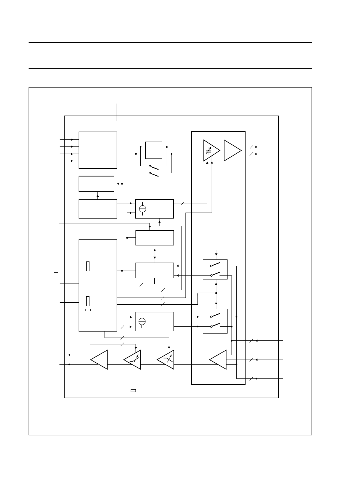
Fig.1 shows the block diagram of the device.
4 ORDERING INFORMATION
TYPE
NUMBER
TDA5155X − naked die −
1997 Apr 08 3
NAME DESCRIPTION VERSION
PACKAGE

Philips Semiconductors Preliminary specification
Pre-amplifier for Hard Disk Drive (HDD)
TDA5155
with MR-read/inductive write heads
5 QUICK REFERENCE DATA
SYMBOL PARAMETER CONDITIONS MIN. TYP. MAX. UNIT
V
CC
V
CC(WD)
G
v(dif)
B
−3dB
F noise figure R
V
irn
CMRR common mode rejection ratio
PSRR power supply rejection ratio
, t
t
r
f
I
MR(PR)
I
WR(b-p)
f
SCLK
supply voltage 4.5 5.0 5.5 V
supply voltage for write drivers V
CC
8.0 8.8 V
differential voltage gain from head inputs to RDx, RDy;
RMR=28Ω; IMR=10mA
data bit d4 = 0 − 160 −
data bit d4 = 1 − 226 −
−3 dB frequency bandwidth upper bandwidth without gain
− 220 − MHz
boost (4 nH lead inductance)
=28Ω; IMR=10mA;
MR
T
=25°C; f = 20 MHz
amb
input referred noise voltage RMR=28Ω; IMR=10mA;
T
=25°C; f = 20 MHz
amb
− 3.0 3.2 dB
− 0.9 1.0 nV/√Hz
IMR=10mA
mismatch <5%
R
MR
f < 1 MHz − 45 − dB
f < 100 MHz − 25 − dB
IMR=10mA
(input referred) R
mismatch <5%
MR
f < 1 MHz − 80 − dB
f < 100 MHz − 50 − dB
write current rise/fall time
(10% to 90%)
programming MR bias current
Lh= 150 nH; Rh=10Ω;
IWR= 35 mA; f = 20 MHz
V
V
R
ext
= 8.0 V −−1.8 ns
CC(WD)
= 6.5 V −−2.1 ns
CC(WD)
=10kΩ 5 − 20.5 mA
range
programming write current range
R
=10kΩ 20 − 51 mA
ext
(base-to-peak)
serial interface clock rate −−25 MHz
1997 Apr 08 4
Philips Semiconductors Preliminary specification
Pre-amplifier for Hard Disk Drive (HDD)
with MR-read/inductive write heads
6 BLOCK DIAGRAM
handbook, full pagewidth
WDlx(i)
WDly(i)
WDlx(v)
WDly(v)
HUS
R
ext
6
7
4
5
3
17
WRITE DRIVER
INPUT
HEAD UNSAFE
INDICATOR
LOW SUPPLY
VOLTAGE
INDICATOR
V
CC
16
TDA5155
FF
WRITE
CURRENT
SOURCE
VOLTAGE
REFERENCE
TDA5155
V
CC(WD)
(5 to 8 V)
1
20, 25, 30, 35,
40, 45, 50, 55,
10
10
10
WRITE DRIVER
AND
READ PREAMP
(10×)
60, 65
19, 24,
29, 34, 39, 44,
49, 54, 59, 64
nWy
nWx
R/W
SCLK
SEN
SDATA
RDx
RDy
+V
CC
8
11
9
10
13
14
SERIAL
INTERFACE
20 kΩ
5
4
4
GNDn
TAS
DETECTOR
4
head select
CURRENT
SOURCE
2, 12, 15, 18
5
3
10
R
MR
23, 28, 33, 38,
43, 48, 53, 58,
10
10
10
63, 68
22, 27, 32, 37,
42, 47, 52, 57,
62, 67
21, 26, 31, 36,
41, 46, 51, 56,
61, 66
MGG982
nRy
nGND
nRx
Fig.1 Block diagram.
1997 Apr 08 5
Philips Semiconductors Preliminary specification
Pre-amplifier for Hard Disk Drive (HDD)
with MR-read/inductive write heads
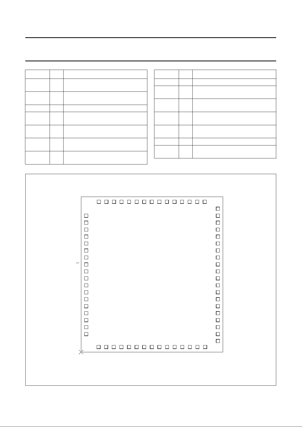
7 PINNING
SYMBOL PAD DESCRIPTION
V
CC(WD)
GND1 2 ground connection 1
HUS 3 head unsafe output
WDIx(v) 4 write data input (differential, voltage
WDIy(v) 5 write data input (differential, voltage
WDIx(i) 6 write data input (differential, current
WDIy(i) 7 write data input (differential, current
R/
W 8 read/write (read = active HIGH,
SEN 9 serial bus enable
SDATA 10 serial bus data
SCLK 11 serial bus clock
GND2 12 ground connection 2
RDx 13 read data output (differential x − y)
RDy 14 read data output (differential x − y)
GND3 15 ground connection 3
V
CC
R
ext
GND4 18 ground connection 4
0Wx 19 inductive write head connection for
0Wy 20 inductive write head connection for
0Rx 21 MR-read head connection for head
0GND 22 ground connection for head H0
0Ry 23 MR-read head connection for head
1Wx 24 inductive write head connection for
1Wy 25 inductive write head connection for
1Rx 26 MR-read head connection for head
1GND 27 ground connection for head H1
1Ry 28 MR-read head connection for head
2Wx 29 inductive write head connection for
1 supply voltage for the write drivers
input)
input)
input)
input)
write = active LOW)
16 supply voltage
17 10 kΩ external resistor
head H0 (differential x − y)
head H0 (differential x − y)
H0 (differential x − y)
H0 (differential x − y)
head H1 (differential x − y)
head H1 (differential x − y)
H1 (differential x − y)
H1 (differential x − y)
head H2 (differential x − y)
TDA5155
SYMBOL PAD DESCRIPTION
2Wy 30 inductive write head connection for
head H2 (differential x − y)
2Rx 31 MR-read head connection for head
H2 (differential x − y)
2GND 32 ground connection for head H2
2Ry 33 MR-read head connection for head
H2 (differential x − y)
3Wx 34 inductive write head connection for
head H3 (differential x − y)
3Wy 35 inductive write head connection for
head H3 (differential x − y)
3Rx 36 MR-read head connection for head
H3 (differential x − y)
3GND 37 ground connection for head H3
3Ry 38 MR-read head connection for head
H3 (differential x − y)
4Wx 39 inductive write head connection for
head H4 (differential x − y)
4Wy 40 inductive write head connection for
head H4 (differential x − y)
4Rx 41 MR-read head connection for head
H4 (differential x − y)
4GND 42 ground connection for head H4
4Ry 43 MR-read head connection for head
H4 (differential x − y)
5Wx 44 inductive write head connection for
head H5 (differential x − y)
5Wy 45 inductive write head connection for
head H5 (differential x − y)
5Rx 46 MR-read head connection for head
H5 (differential x − y)
5GND 47 ground connection for head H5
5Ry 48 MR-read head connection for head
H5 (differential x − y)
6Wx 49 inductive write head connection for
head H6 (differential x − y)
6Wy 50 inductive write head connection for
head H6 (differential x − y)
6Rx 51 MR-read head connection for head
H6 (differential x − y)
6GND 52 ground connection for head H6
6Ry 53 MR-read head connection for head
H6 (differential x − y)
7Wx 54 inductive write head connection for
head H7 (differential x − y)
1997 Apr 08 6
Philips Semiconductors Preliminary specification
Pre-amplifier for Hard Disk Drive (HDD)
with MR-read/inductive write heads
SYMBOL PAD DESCRIPTION
7Wy 55 inductive write head connection for
head H7 (differential x − y)
7Rx 56 MR-read head connection for head
H7 (differential x − y)
7GND 57 ground connection for head H7
7Ry 58 MR-read head connection for head
H7 (differential x − y)
8Wx 59 inductive write head connection for
head H8 (differential x − y)
8Wy 60 inductive write head connection for
head H8 (differential x − y)
8Rx 61 MR-read head connection for head
H8 (differential x − y)
handbook, full pagewidth
9Wx
9GND
9Rx
9Wy
8Ry
9Ry
TDA5155
SYMBOL PAD DESCRIPTION
8GND 62 ground connection for head H8
8Ry 63 MR-read head connection for head
H8 (differential x − y)
9Wx 64 inductive write head connection for
head H9 (differential x − y)
9Wy 65 inductive write head connection for
head H9 (differential x − y)
9Rx 66 MR-read head connection for head
H9 (differential x − y)
9GND 67 ground connection for head H9
9Ry 68 MR-read head connection for head
H9 (differential x − y)
7Wx
7Wy
7Rx
7GND
7Ry
8Wx
8Wy
8Rx
8GND
V
CC(WD)
GND1
WDIx(v)
WDIy(v)
WDIx(i)
WDIy(i)
SDATA
SCLK
GND2
GND3
GND4
HUS
R/W
SEN
RDx
RDy
V
CC
R
ext
6465666768 54555657585960616263
1
2
3
4
5
6
7
8
9
10
11
12
13
14
15
16
17
18
19 20 21 22 23 24 25 26 27 28 29 30 31 32 33
TDA5155
6Ry
53
52
6GND
51
6Rx
50
6Wy
49
6Wx
48
5Ry
47
5GND
46
5Rx
45
5Wy
44
5Wx
43
4Ry
42
4GND
41
4Rx
40
4Wy
39
4Wx
38
3Ry
37
3GND
36
3Rx
35
3Wy
34
3Wx
0
0Wx
0Wy
0Rx
0GND
0Ry
1Wx
1Wy
Fig.2 Pad arrangement.
1997 Apr 08 7
1Rx
1GND
1Ry
2Wx
2Wy
2Rx
2GND
2Ry
MGG981

Philips Semiconductors Preliminary specification
Pre-amplifier for Hard Disk Drive (HDD)
with MR-read/inductive write heads
8 FUNCTIONAL DESCRIPTION
8.1 Read mode
The read mode disables the write circuitry to save power
while reading. The read circuitry is disactivated for write,
sleep and standby modes. The read circuitry may also be
biased during write mode to shorten transients.
The selected head is connected to a multiplexed low-noise
read amplifier. The read amplifier has low-impedance
inputs nRx and nRy (n is the number of the head) and
low-impedance outputs RDx and RDy. The signal polarity
is non-inverting from x and y inputs to x and y outputs.
Ambient magnetic fields at the MR elements result in a
relative change in MR resistance:
dR
MR
-------------R
MR
This change produces a current variation:
dR
dI
MRIMR
where I
MR
The current variation is amplified to form the read data
output signal voltage, which is available at RDx and RDy.
AC coupling between MR elements and amplifier stages
prevents the amplifier input stages from overloading by DC
voltages across the MR elements. A fast settling
procedure shortens DC settling transients.
MR
×=
-------------R
MR
,
is the bias current in the MR element.
TDA5155
8.2 Write mode
To minimize power dissipation, the read circuitry may be
disabled in write mode. The write circuitry is disabled in
read, sleep and standby modes. In write mode, a
programmable current is forced through the selected
two-terminal inductive write head. The push-pull output
drivers yield near rail-to-rail voltage swings for fast current
polarity switching.
The write data input can be either voltage or current input
(see Chapter 12). In voltage mode, the differential write
data inputs WDIx(v) and WDIy(v) are PECL (Positive
Emitter Coupled Logic) compatible. The write data flip-flop
can either be used or passed-by. In the case that the write
data flip-flop is used, current polarity is toggled at the
falling edges of
V
V
data
WDIx v()VWDIy v()
=
------------------------------------------------------
Switching to write mode initializes the data flip-flop so that
the write current flows in the write head from x to y. In the
case that the write data flip-flop is not used, the signal
polarity is non-inverting from x and y inputs to
x and y outputs.
The write current magnitude is controlled through on-chip
DACs. The write current is defined as follows:
10kΩ
I
-------------- -
WR
R
ext
–
2
20 16d4 8d3 4d2 2d1 d0+++++()=
An on-chip generated stable temperature reference
voltage (1.32 V), available at the R
pin, is dropped
ext
across an external resistor (10 kΩ) to form a global
reference current for the write and the MR bias currents.
The MR bias current DACs are programmed through the
serial interface according to the following formula:
10kΩ
I
MR
0.5
10 16d4 8d3 4d2 2d1 d0+++++()×=
-------------- R
ext
(in mA), where d4-d0 are bits (either logic 0 or logic 1).
At power-up all bits are set to logic 0, which results in a
default MR current of 5 mA. The adjustable range of the
MR currents is 5 mA to 20.5 mA. The MR bias currents are
equal for the two stripes of each head. The gain amplifier
is 1-bit programmable. The amplifier gain can be set to its
nominal value or to the nominal value +3 dB.
(in mA), where d4-d0 are bits (either logic 0 or logic 1).
The adjustable range of the write current is 20 mA to
51 mA. At power-up, the default values
d4 = d3 = d2 = d1 = d0 = logic 0 are initialized,
corresponding to I
= 20 mA. IWR is the current provided
WR
by the write drivers: the current in the write coil and in the
damping resistor together. The static current in the write
coil is
I
WR
,
---------------- R
h
1
+
------ R
d
where R
R
d
is the resistance of the coil including leads and
h
is the damping resistor.
1997 Apr 08 8
 Loading...