

Philips tda3842 DATASHEETS

INTEGRATED CIRCUITS
DATA SH EET
TDA3842
Multistandard TV IF amplifier and
demodulator with TV signal
identification
Preliminary specification
File under Integrated Circuits, IC02
April 1991

Philips Semiconductors Preliminary specification
Multistandard TV IF amplifier and
TDA3842
demodulator with TV signal identification
FEATURES
• Low supply voltage range, from 5.0 V to 8.0 V
• Low power dissipation, 200 mW at 5 V
• High supply ripple rejection
• Wide IF bandwidth of 80 MHz
• Synchronous demodulator with low differential phase
and gain
• Additional video buffer with a wide bandwidth of 10 MHz
• Video off switch
• Peak sync AGC for negative modulation, e.g. B/G
• Peak white AGC for positive modulation, e.g. L
QUICK REFERENCE DATA
SYMBOL PARAMETER CONDITIONS MIN. TYP. MAX. UNIT
V
P
I
P
V
1-20(rms)
supply voltage range (pin 15) 4.75 5.0 8.8 V
supply current (pin 15) VP= 5.0 V − 42 − mA
IF input signal for nominal video output
voltage at pin 14 (RMS value)
minimum IF input signal for TV signal
identification at pin 6 (RMS value)
V
o
G
v
video output signal (pin 12) buffered − 2.0 − V
IF voltage gain control range − 66 − dB
S/N signal-to-noise ratio V
V
S
8
AFC
AFC output voltage swing − 4.0 − V
AFC steepness (pin 8) − 2 −µA/kHz
RR supply voltage ripple rejection (pin 12) 30 35 − dB
• Adjustable take-over point (TOP); positive AGC slope
• Switching to fast AGC dependent on TV identification
• Alignment free AFC detector with integrated phase shift
• ESD protection
• TV signal identification
• Options: tracking of reference circuit, suitable for
MAC-on-cable
GENERAL DESCRIPTION
The TDA3842 is a bipolar integrated circuit for vision
IF-signal processing in multistandard TV and VTRs,
designed for a supply voltage range from 5.0 V to 8.0 V.
f = 38.9 MHz − 70 −µV
maximum G
=10mV 55 60 − dB
1-20
− 20 40 µV
v
ORDERING INFORMATION
EXTENDED
TYPE NUMBER
TDA3842 20 DIL plastic SOT146
TDA3842T 20 mini-pack plastic SO20L; SOT163A
Notes
1. SOT146-1; 1997 January 08.
2. SOT163-1; 1997 January 08
April 1991 2
PACKAGE
PINS PIN POSITION MATERIAL CODE
(1)
(2)
Philips Semiconductors Preliminary specification
Multistandard TV IF amplifier and
demodulator with TV signal identification
TDA3842
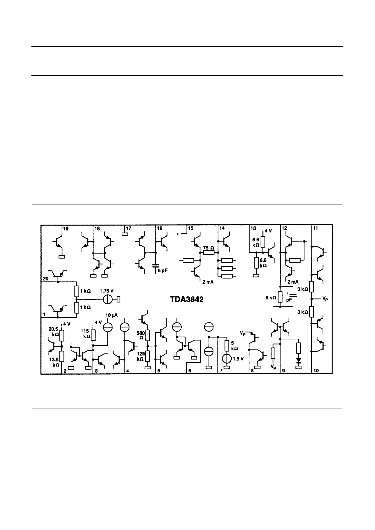
PIN CONFIGURATION
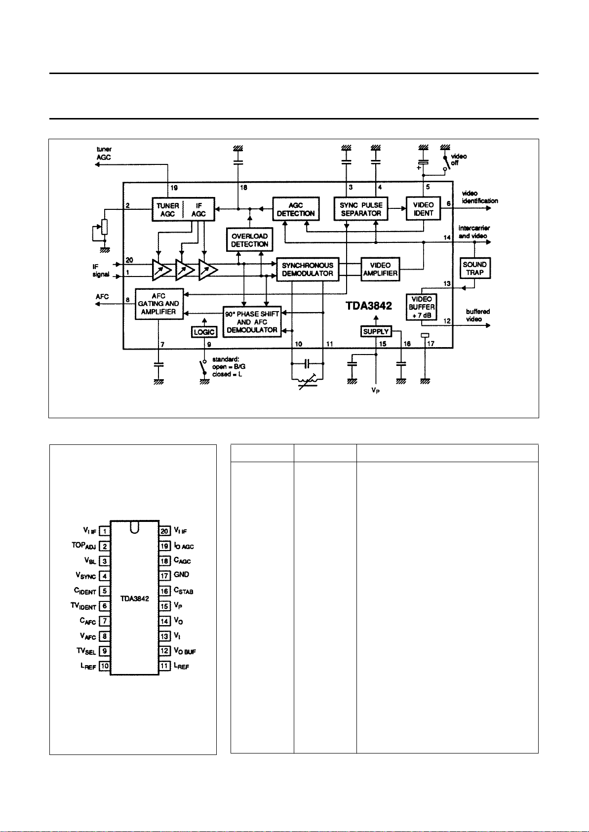
Fig.2 Pin configuration.
Fig.1 Block diagram.
PINNING
SYMBOL PIN DESCRIPTION
v
I IF
TOP
v
BL
V
SYNC
C
IDENT
TV
C
AFC
V
AFC
TV
L
REF
L
REF
v
O BUF
v
I
v
O
v
P
C
STAB
ADJ
IDENT
SEL
1 IF input (balanced)
2 tuner AGC take-over point adjustment
3 black level voltage
4 sync pulse amplitude voltage
5 identification capacitor
6 video identification output
7 AFC capacitor
8 AFC output signal
9 video standard selection switch
10 LC reference tuned circuit
11 LC reference tuned circuit
12 buffered video output signal
13 video input signal for buffer
14 video output signal with intercarrier signal
15 supply voltage
16 supply voltage stabilization
GND 17 ground
C
AGC
I
O AGC
v
I IF
18 AGC capacitor
19 tuner AGC output signal
20 IF input (balanced)
April 1991 3

Philips Semiconductors Preliminary specification
Multistandard TV IF amplifier and
demodulator with TV signal identification
FUNCTIONAL DESCRIPTION
The complete circuit consists of the
following functional blocks as shown
in Fig.1:
1. 3-stage gain controlled IF
amplifier
2. Overload detector
3. Reference amplifier
4. Carrier signal reference limiter
5. Video demodulator
6. Video amplifier
7. Video buffer amplifier
8. AGC detector
9. IF and tuner AGC (with
adjustable TOP)
10. Sync pulse separator
11. Video identification
12. 90°phase shift and AFC
demodulator
13. AFC gating, AFC amplifier and
AFC switch
14. Voltage stabilizer
15. Standard switch
1. 3-stage gain controlled IF
amplifier (pins 1 and 20)
The vision IF amplifier consists of
three AC-coupled differential
amplifier stages. Gain control is
achieved by current divider stages.
The emitter feedback resistors are
optimized for low noise and signal
handling capability.
2. Overload detector
The overload detector is fed from the
output of the third IF amplifier. As
soon as the IF voltage exceeds the
overload threshold in the detector, its
output current reduces the IF
amplification by discharging the AGC
capacitor.
3. Reference amplifier
For passive video carrier
regeneration an integrated differential
amplifier with resistive load allows
capacitive coupling of the resonant
circuit for notch and tracking
functions.
4. Carrier signal reference limiter
A limiter stage after the reference
amplifier eliminates amplitude
modulation. Its output is fed to the
video demodulator.
5. Video demodulator
The video demodulator receives both
the limited reference carrier signal
and the IF signal. The video signal
polarity is switched according to the
TV standard selected. The video
signal can also be switched off.
6. Video amplifier
The video amplifier is an operational
amplifier with internal feedback and
wide bandwidth. The DC level is
shifted according to the TV standard
to provide the same sync level for
positive and negative IF modulation.
7. Video buffer amplifier
The video buffer amplifier is an
operational amplifier with internal
feedback, wide bandwidth and
frequency compensation; gain and
input impedance are adapted to
operate with a ceramic sound trap.
The load for the sound trap is an
integrated resistive divider.
8. AGC detector
With negative modulation
peak sync AGC detector generates a
fast current pulse to discharge the
AGC capacitor (gain reduction). This
minimizes the video signal distortion.
Positive modulation
white AGC detector.
To filter out the sound carrier the
video signal is fed through low pass
filters. After the low pass filters the
video signal with attenuated sound
carrier, is fed to the AGC detector.
(B/G) a
(L) uses a peak
TDA3842
The charging current of the AGC
capacitor is optimized for minimum
distortion of the video signal. With
positive modulation the charging
current is very low and consequently
the AGC time constant is large. When
the video identification circuit does
not detect a video signal, the charging
current is increased.
9. IF and tuner AGC
The voltage on the AGC capacitor is
used to control the gain of the three IF
amplifier stages and to supply the
tuner AGC current (open-collector).
The tuner AGC TOP potentiometer at
pin 2 adjusts the IF signal level from
the tuner. To stabilize the IF output
voltage of the tuner, IF slip
(= variation of IF gain over the total
tuner range) is kept at a minimum.
10. Sync pulse separator
The sync pulse separator supplies
two internally-used pulses using the
bandwidth limited video signal. These
are the composite sync for the AFC
detector and the vertical sync for the
video identification output. The
bandwidth is limited to reduce the
noise and increase the ident
sensitivity.
11. Video identification
An analog integrator monitors the
duty cycle of the vertical sync pulses
to identify the video signal. The
integrator output is fed to a window
comparator which has an open
collector output stage to provide the
video ident signal. The complete
circuit operates in combination with
the sync separator and is optimized
for high sensitivity.
12. 90° phase shift and AFC
demodulator
The AFC demodulator needs a 90°
phase-shifted carrier. The output of
the carrier signal reference limiter is
April 1991 4
Philips Semiconductors Preliminary specification
Multistandard TV IF amplifier and
demodulator with TV signal identification
fed to an active 90° phase-shift circuit.
The 90° (lead) phase-shifted carrier
and the IF signal are fed to the AFC
demodulator. The demodulated
signal is fed to the AFC gating stage.
13. AFC gating, AFC amplifier and
AFC switch
With negative modulated video IF
signals the output of the AFC detector
is gated by composite sync pulses to
prevent video modulation on the AFC
output. The gated signal is integrated
by an AFC capacitor. The AFC
amplifier converts the capacitor
voltage to an AFC current (open
collector sink/source output). At
positive modulation the AFC operates
continuously.
AFC function can be externally
switched off for test purposes. For
high-performance signal handling the
AFC signal can be used to track the
resonant circuit as shown in Fig.11.
TDA3842
14. Voltage stabilizer
An integrated bandgap voltage
stabilizer generates an internal
supply voltage of 4 V. A decoupling
capacitor reduces noise and supply
voltage ripple.
15. Standard switch
The operating mode of the AGC
detector and video IF demodulator for
positive and negative IF modulation is
selected by the logic level on pin 9.
April 1991 5
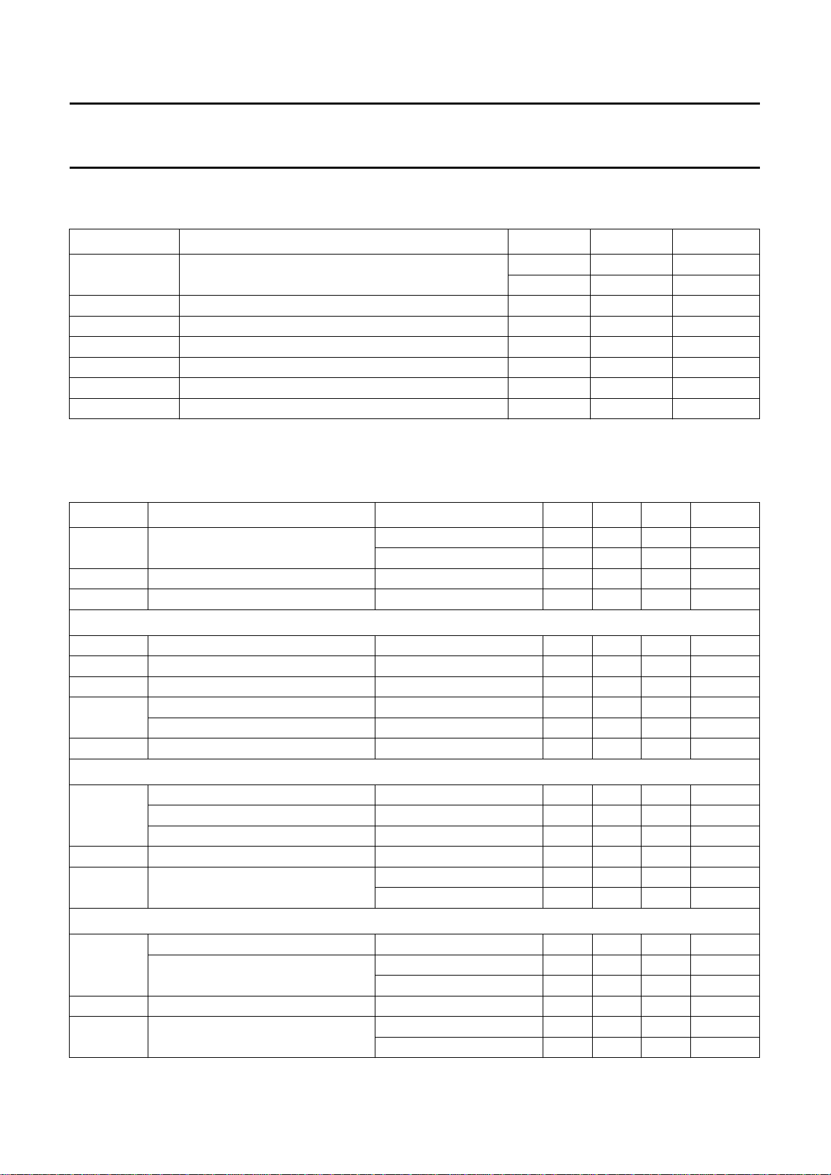
Fig.3 Internal circuits.
Philips Semiconductors Preliminary specification
Multistandard TV IF amplifier and
TDA3842
demodulator with TV signal identification
LIMITING VALUES
In accordance with the Absolute Maximum System (IEC 134)
SYMBOL PARAMETER MIN. MAX. UNIT
v
p
v
19
v
8
I
15
T
stg
T
amb
v
ESD
CHARACTERISTICS
= 5 V and T
V
P
Fig.4.; unless otherwise specified.
SYMBOL PARAMETER CONDITIONS MIN. TYP. MAX. UNIT
V
P
I
P
RR ripple rejection (pin 12) 30 35 − dB
supply voltage at pin 15: SOT146 − 8.8 V
SOT163A − 6.0 V
tuner AGC voltage − 13.2 V
permissible voltage at AFC output − V
P
V
supply current − 55 mA
storage temperature range −25 + 150 °C
operating ambient temperature range 0 + 70 °C
ESD sensitivity −±300 V
=25°C; fVC= 38.9 MHz; all voltages are measured to GND (pin 17); measured in test circuit of
amb
supply voltage range (pin 15) DIL-package 4.75 5.0 8.8 V
SO-package 4.75 5.0 6.0 V
supply current (pin 15) VP= 5.0 V − 42 − mA
IF amplifier
B bandwidth −3dB − 80 − MHz
R
I
C
I
V
1-20(rms)
G
v
input resistance (pins 1 and 20) − 2 − kΩ
input capacitance (pins 1 and 20) − 1.5 − pF
IF input signal (RMS value) video output −1dB − 70 −µV
maximum IF input signal minimum G
; note 1 100 −−mV
v
gain control range 63 66 − dB
IF AGC: negative modulation
I
18
leakage current AGC capacitor −−1µA
charging current AGC capacitor with video identification − 13 −µA
charging current AGC capacitor without video identification − 35 −µA
I
18M
t
1
discharging peak current capacitor − 2 − mA
response time of IF input signal
change
50 dB increasing step − 1 − ms
50 dB decreasing step − 150 − ms
IF AGC: standard L (note 2)
I
18
leakage current AGC capacitor −−20 nA
charging current AGC capacitor with video identification − 280 − nA
without video identification − 22 −µA
I
18M
t
2
discharging peak current capacitor − 2 − mA
response time of IF input signal
change
50 dB increasing step − 1 − ms
50 dB decreasing step − 300 − ms
April 1991 6
 Loading...