

Philips tda3833 DATASHEETS
INTEGRATED CIRCUITS
DATA SH EET
TDA3833
BTSC-stereo/SAP/DBX decoder
and DBX expander
Product specification
File under Integrated Circuits, IC02
September 1992

Philips Semiconductors Product specification
BTSC-stereo/SAP/DBX decoder and DBX expander TDA3833
FEATURES
• DBX decoder, MPX decoder
and SAP decoder on chip
• Extensive switching
possibilities for the AF outputs
and the extra headphone
output
• Stereo and SAP signal
available simultaneously
• Reliable stereo/SAP
identification by means of the
noise detector
• Integrated filters
• DAC control possible for most
alignments
• Few external components
• Low power consumption
(200 mW)
•+5 V supply voltage
GENERAL DESCRIPTION
QUICK REFERENCE DATA
SYMBOL PARAMETER TYP. UNIT
V
P
I
P
V
i
positive supply voltage (pin 32) 5 V
supply current 42 mA
input signal, 100% modulated, mono
100 mV
(RMS value, pin 1)
V
o
AF output signal (RMS value, pins 7, 23 and 24) 550 mV
S/N(W) signal-to-noise ratio, weighted 50 dB
S/N signal-to-noise ratio 60 dB
α
CH
α
CR
stereo channel separation 26 dB
crosstalk attenuation 60 dB
THD total harmonic distortion 0.2 %
ORDERING INFORMATION
PACKAGE
EXTENDED
TYPE NUMBER
PINS
TDA3833 32 SDIL plastic SOT232AG
TDA3833T 32 SO plastic SOT287AH
PIN
POSITION
MATERIAL CODE
(1)
(2)
The TDA3833 is a sound
processor for stereo/second
audio program (SAP) baseband
signals in accordance with the
BTSC standard for television
receivers and video tape
recorders.
Note
1. SOT232-1; 1996 December 13.
2. SOT287-1; 1996 December 13.
September 1992 2
Philips Semiconductors Product specification
BTSC-stereo/SAP/DBX decoder and DBX
expander
TDA3833
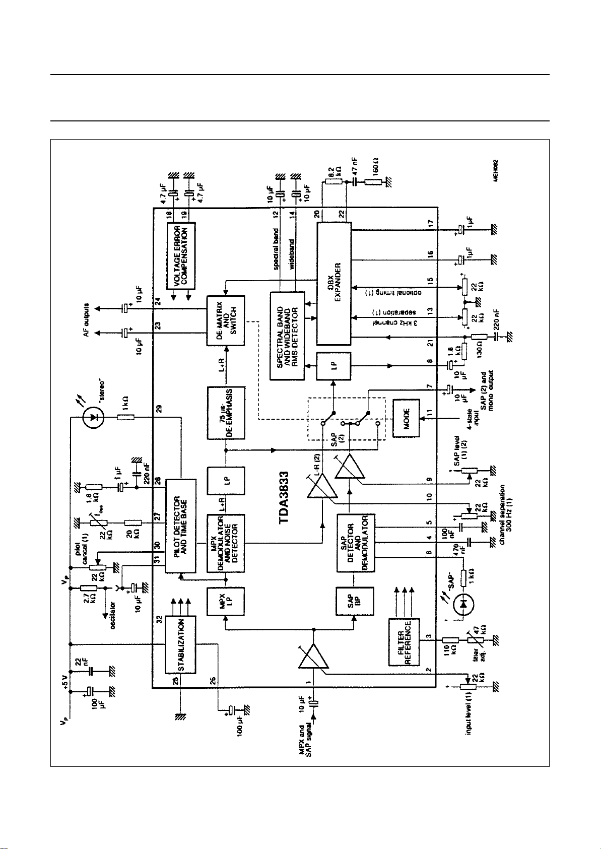
(1) control possible by DAC
(2) DBX encoded
Fig.1 Block diagram, test and application circuit.
September 1992 3
Philips Semiconductors Product specification
BTSC-stereo/SAP/DBX decoder and DBX expander TDA3833
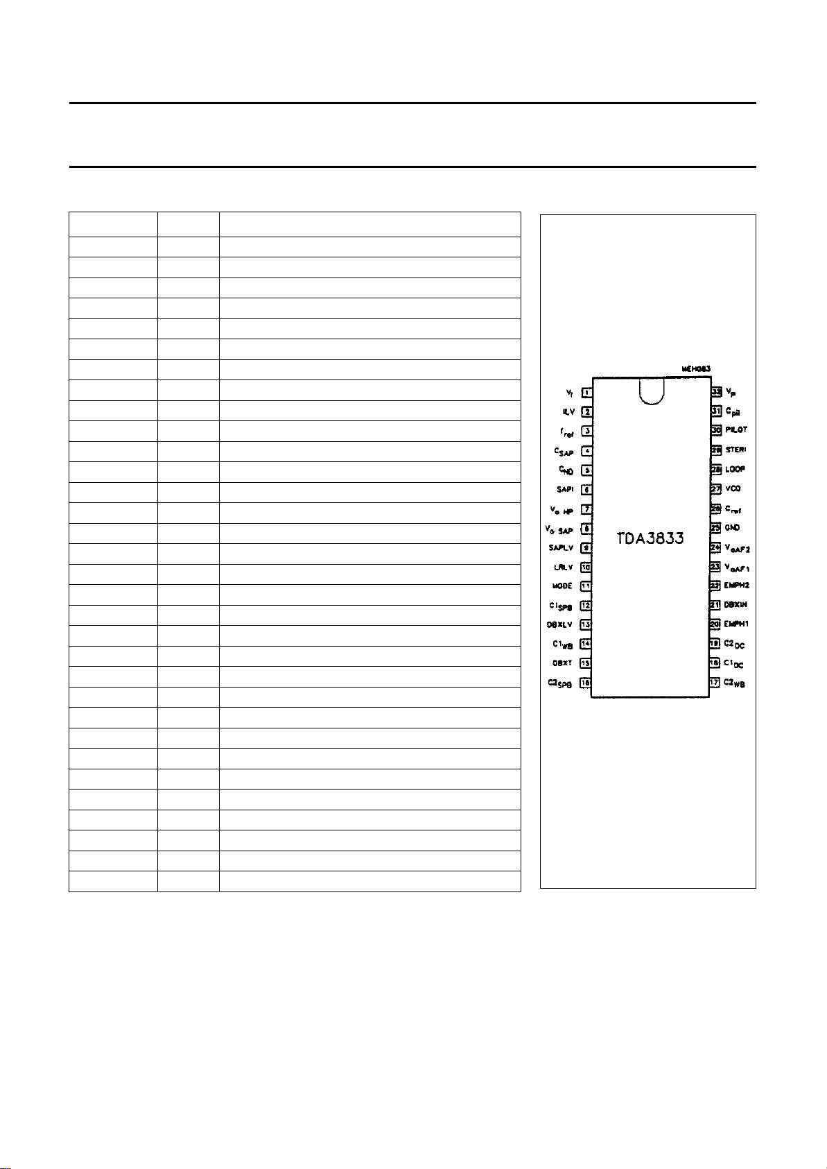
PINNING
SYMBOL PIN DESCRIPTION
V
i
ILV 2 input level control
f
ref
C
SAP
C
ND
SAPI 6 SAP indicator output (sink)
V
oHP
V
o SAP
SAPLV 9 SAP level control
LRLV 10 (L-R) level control
MODE 11 4-state mode control
C1
SPB
DBXLV 13 DBX spectral adjust
C1
WB
DBXT 15 DBX timing adjust
C2
SPB
C2
WB
C1
DC
C2
DC
EMPH1 20 time constant for variable emphasis
DBXIN 21 DBX signal input
EMPH2 22 time constant for variable emphasis
V
oAF1
V
oAF2
GND 25 ground (0 V)
C
ref
VCO 27 VCO free running frequency adjustment
LOOP 28 phase detector loop filter
STERI 29 stereo indicator output (sink)
PILOT 30 pilot cancel adjustment
C
pil
V
P
1 composite input signal (MPX/SAP)
3 adjustment of filter reference
4 SAP identity smoothing capacitor
5 SAP noise detector smoothing capacitor
7 SAP/mono headphone output
8 output signal SAP/(L-R) without DBX
12 spectral band timing capacitor
14 wideband timing capacitor
16 spectral RMS-detector smoothing capacitor
17 wideband RMS-detector smoothing capacitor
18 DC decoupling capacitor 1 for offset compensation
19 DC decoupling capacitor 2 for offset compensation
23 AF output signal right/SAP or mono
24 AF output signal left/SAP or mono
26 smoothing capacitor for internal reference voltage
31 pilot detector smoothing capacitor, VCO/4 output
32 +5 V supply voltage
Fig.2 Pin configuration.
September 1992 4
 Loading...