

Philips TDA3803A Datasheet

INTEGRATED CIRCUITS
DATA SH EET
TDA3803A
Stereo/dual TV sound decoder
circuit
Product specification
File under Integrated Circuits, IC02
November 1987

Philips Semiconductors Product specification
Stereo/dual TV sound decoder circuit TDA3803A
GENERAL DESCRIPTION
The TDA3803A is a stereo/dual TV sound decoder circuit with static switching for processing two AF signals in TV and
VCR equipment. The LOW/HIGH static switching signals control the AF output selector. Two operational amplifiers
perform bandpass filtering of the identification signals.
Features
• Amplification of the two AF input signals by integrated operational amplifiers
• Low distortion stereo de-matrix
• All operational amplifiers offset compensated
• De-emphasis with operational amplifiers, preferably applied to the output terminals
• Two output ports each with two channels for headphones and loudspeakers
• Dual sound information at one port, each port individually switchable from sound I to sound II and sound II to sound I
• Mute function; while mute is active, it is possible to connect an external mono AF input signal to pin 10 appearing at
pins 20 to 23.
• Identification without additional signals (horizontal etc.)
QUICK REFERENCE DATA
Supply voltage (pin 13) V
Supply current (pin 13) I
P=I13
Pilot carrier amplifier gain control range ∆G
A.F. input signals; at G
=0dB
v
(r.m.s. value) V
LED output current I
LED
P=V13-12
v
i(rms)
typ. 12 V
typ. 28 mA
> 40 dB
=1V
typ. 12 mA
Weighted signal-to-noise ratio
of the a.f. signal switches (CCIR468/2) (S+N)/N ≥ 60 dB
Crosstalk in stereo mode α
Crosstalk in dual sound mode α
S
DS
> 40 dB
> 60 dB
PACKAGE OUTLINE
28-lead DIL; plastic (SOT117); SOT117-1; 1996 November 25.
November 1987 2
Philips Semiconductors Product specification
Stereo/dual TV sound decoder circuit TDA3803A
November 1987 3
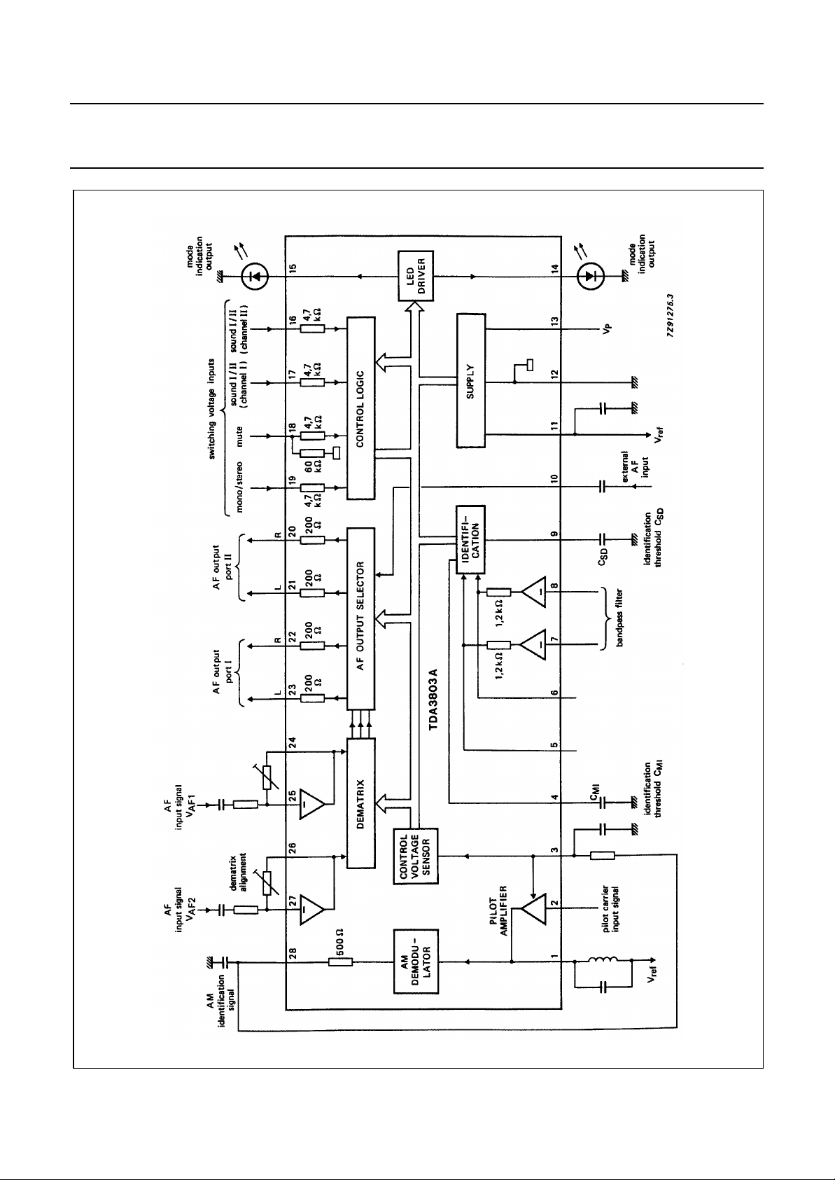
Fig.1 Block diagram.

Philips Semiconductors Product specification
Stereo/dual TV sound decoder circuit TDA3803A
RATINGS
Limiting values in accordance with the Absolute Maximum System (IEC 134)
Supply voltage (pin 13) V
Voltages with respect to pin 12 (ground)
pins 25; 27 and 28 V
Voltages
pin 1 to pin 10 V
pin 14 to pin 19 V
Currents
pin 11 I
pins 20; 21; 22; 23 I
pin 28 −I
Total power dissipation P
Storage temperature range T
Operating ambient temperature range T
P=V13-12
25; 27; 28-12
n-12
n-12
11
20;21;22;23
28
tot
stg
amb
max. 14 V
max. V
max. V
max. V
P
P
P
max. 3 mA
max. 10 mA
max. 3 mA
max. 1,5 W
−25 to + 125 °C
0 to + 70 °C
November 1987 4
 Loading...