

Philips TDA3661AT Datasheet

INTEGRATED CIRCUITS
DATA SH EET
TDA3661
Very low dropout voltage/quiescent
current adjustable voltage regulator
Product specification
Supersedes data of 2000 Dec 08
File under Integrated Circuits, IC01
2000 Dec 13
Philips Semiconductors Product specification
Very low dropout voltage/quiescent current
TDA3661
adjustable voltage regulator
FEATURES
• Output adjustable from 1.5 V to VP, 100 mA regulator
• Supply voltage range up to 45 V
• Very low quiescent current of 15 µA (typical value)
• Very low dropout voltage
• High ripple rejection
• Very high stability:
– Electrolytic capacitors: Equivalent Series
Resistance (ESR) < 22 Ω at worst-case condition
– Other capacitors: 100 nFat 200 µA ≤ I
REG
≤ 100 mA.
• Pin compatible family TDA3662 to TDA3666
• Protections:
QUICK REFERENCE DATA
SYMBOL PARAMETER CONDITIONS MIN. TYP. MAX. UNIT
– Reverse polarity safe (down to −25 V without high
reverse current)
– Negative transient of 50 V (RS=10Ω, t < 100 ms)
– Able to withstand voltages up to 18 V at the output
(supply line may be short-circuited)
– ESD protection on all pins
– DC short-circuit safe to ground and VP of the
regulator output
– Temperature protection (at Tj> 150 °C).
GENERAL DESCRIPTION
The TDA3661 is an adjustable voltage regulator with very
lowdropout voltage andquiescentcurrent, which operates
over a wide supply voltage range.
Supply
V
P
I
q
supply voltage regulator on 3 14.4 45 V
quiescent supply current VP= 14.4 V; I
=0mA − 15 30 µA
REG
Regulator; k = 4.01929 (note 1)
V
REG
V
ref
V
REG(drop)
output voltage 8 V ≤ VP≤ 22 V; I
6V≤V
V
P
0.5 mA ≤ I
≤45 V; I
P
= 14.4 V;
REG
≤ 100 mA
reference voltage VP= 14.4 V 1.181 1.244 1.306 V
dropout voltage VP= 4.5 V; I
T
amb
REG
≤ 85 °C
= 0.5 mA 4.8 5.0 5.2 V
REG
= 0.5 mA 4.75 5.0 5.25 V
REG
4.75 5.0 5.25 V
= 50 mA;
− 0.18 0.3 V
Note
1.
V
REG
V
k×=
ref
ORDERING INFORMATION
TYPE
NUMBER
NAME DESCRIPTION VERSION
PACKAGE
TDA3661AT SO8 plastic small outline package; 8 leads; body width 3.9 mm SOT96-1
2000 Dec 13 2
Philips Semiconductors Product specification
Very low dropout voltage/quiescent current
adjustable voltage regulator
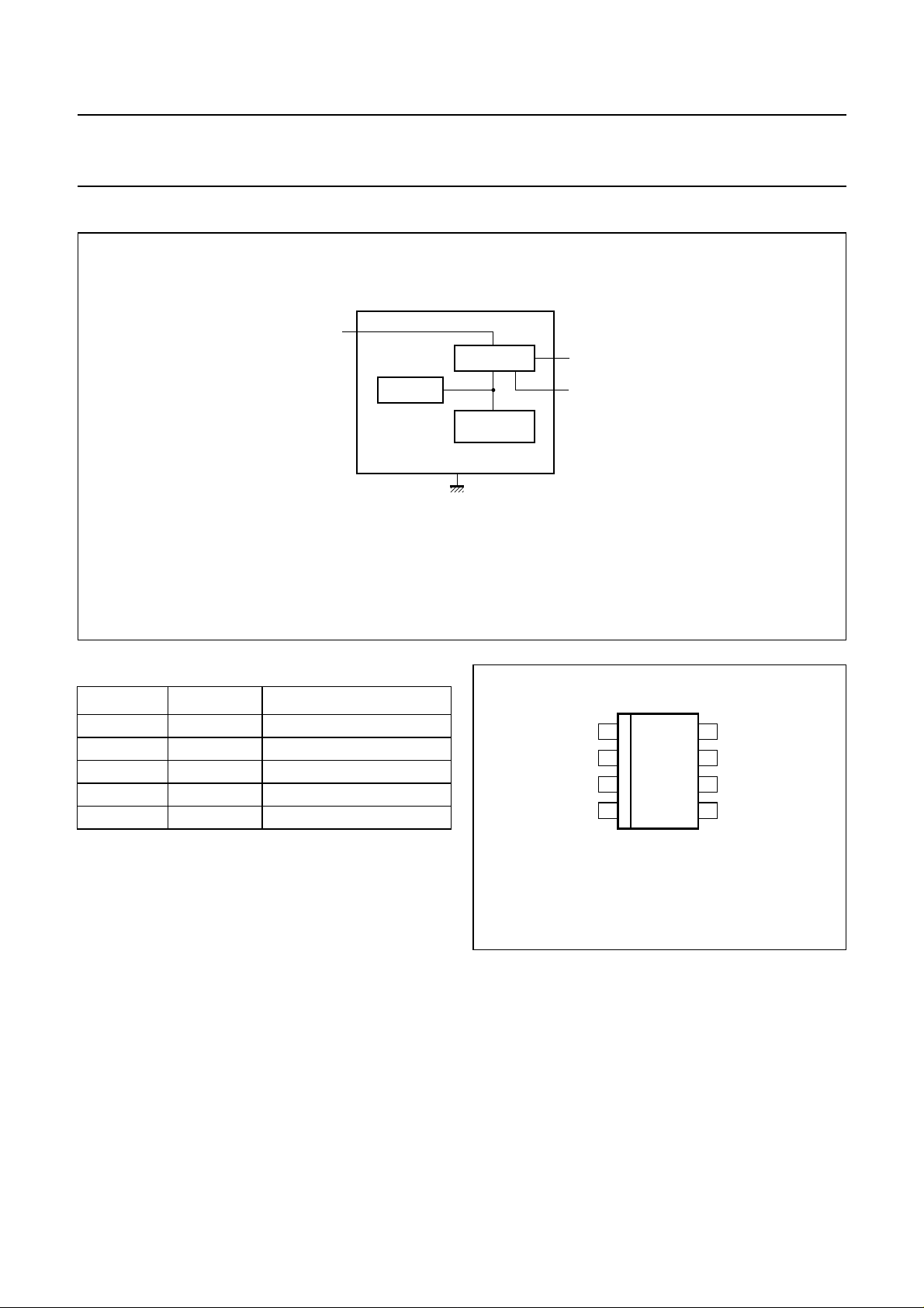
BLOCK DIAGRAM
handbook, halfpage
8
V
P
REGULATOR
BAND GAP
TDA3661
PROTECTION
2, 3, 6, 7
GND
THERMAL
MGS579
TDA3661
1
REG
5
ADJ
Fig.1 Block diagram.
PINNING
SYMBOL PIN DESCRIPTION
REG 1 regulator output
GND 2, 3, 6 and 7 ground; note 1
n.c. 4 not connected
ADJ 5 feedback input
V
P
8 supply voltage
Note
1. All GND pins are connected to thelead frameand can
also be used to reduce the total thermal resistance
by soldering these pins to a ground plane.
R
th(j-a)
The ground plane on the top side of the PCB acts like
a heat spreader.
handbook, halfpage
REG
1
2
TDA3661
3
GND
4
n.c.
MGS580
Fig.2 Pin configuration.
V
8
P
GNDGND
7
GND
6
ADJ
5
2000 Dec 13 3
Philips Semiconductors Product specification
Very low dropout voltage/quiescent current
TDA3661
adjustable voltage regulator
FUNCTIONAL DESCRIPTION
The TDA3661 is an adjustable voltage regulator with an
output voltage that can be fixed by means of an external
resistor divider. The regulator can deliver output currents
up to 100 mA. The regulator is available in an SO8
package. The regulator is intended for portable, mains,
telephone and automotive applications. To increase the
lifetime of batteries, aspecially built-in clamp circuit keeps
the quiescent current of this regulator very low, in dropout
and full load conditions.
The device remains operational down to very low supply
voltages (typical 2 V) and belowthis voltageit switchesoff.
LIMITING VALUES
In accordance with the Absolute Maximum Rating System (IEC 60134).
SYMBOL PARAMETER CONDITIONS MIN. MAX. UNIT
V
V
P
T
T
T
P
P(rp)
tot
stg
amb
j
supply voltage − 45 V
reverse polarity supply voltage non-operating −−25 V
total power dissipation temperature of copper area
storage temperature non-operating −55 +150 °C
ambient temperature operating −40 +125 °C
junction temperature operating −40 +150 °C
Atemperatureprotection is includedwhich switchesoff the
regulator output at a junction temperature above 150 °C.
A new output circuit guarantees the stability of the
regulator for a capacitor output circuit with an ESR
(worst-case) up to22 Ω, seeFigs 4 and 5. If only a 100 nF
capacitor is used, the regulator is fully stable when
I
> 200 µA. This is very attractive as the ESR of an
REG
electrolytic capacitor increases strongly at low
temperatures (no expensive tantalum capacitor is
required).
− 4.1 W
is 25 °C
THERMAL CHARACTERISTICS
SYMBOL PARAMETER CONDITIONS VALUE UNIT
R
R
th(j-c)
th(j-a)
thermal resistance from junction to case to centre pins; soldered 30 K/W
thermal resistance from junction to ambient in free air; soldered 125 K/W
QUALITY SPECIFICATION
In accordance with
“SNW-FQ-611E”
.
2000 Dec 13 4
Philips Semiconductors Product specification
Very low dropout voltage/quiescent current
TDA3661
adjustable voltage regulator
CHARACTERISTICS
VP= 14.4 V; T
SYMBOL PARAMETER CONDITIONS MIN. TYP. MAX. UNIT
Supply voltage: pin V
V
P
I
q
Regulator output: pin REG
V
REG
V
REG(drop)
V
REG(stab)
V
REG(adj)
∆V
REG(line)
∆V
REG(load)
SVRR supply voltage ripple rejection f
V
ref
I
REG(crl)
I
LO(rp)
=25°C; k = 4.01929 (note 1); measured with test circuit of Fig.3; unless otherwise specified.
amb
P
supply voltage regulator operating; note 2 3 14.4 45 V
quiescent supply current VP= 4.5 V; I
V
= 14.4 V; I
P
6V≤V
6V≤V
≤24 V; I
P
≤24 V; I
P
output voltage 8 V ≤ VP≤ 22 V; I
0.5 mA ≤ I
6V≤V
≤45 V; I
P
dropout voltage VP= 4.5 V; T
I
=50mA
REG
=0mA − 10 30 µA
REG
=0mA − 15 30 µA
REG
=10mA − 0.2 0.5 mA
REG
=50mA − 1.4 2.5 mA
REG
= 0.5 mA 4.8 5.0 5.2 V
REG
≤ 100 mA 4.75 5.0 5.25 V
REG
= 0.5 mA 4.75 5.0 5.25 V
REG
amb
≤ 85 °C;
− 0.18 0.3 V
output voltage long-term stability − 20 − mV/1000 h
output voltage adjust range 1.5 − V
line input regulation voltage 7 V ≤ VP≤ 22 V; I
7V≤V
load output regulation voltage 0.5 mA ≤ I
= 120 Hz;
i
V
i(ripple)
I
REG
≤45 V; I
P
REG
= 1 V (RMS);
= 0.5 mA
≤ 50 mA − 10 50 mV
= 0.5 mA − 130mV
REG
= 0.5 mA − 150mV
REG
50 60 − dB
V
P
reference voltage VP= 14.4 V 1.181 1.244 1.306 V
output current limit V
output leakage currentat reverse
> 4 V 0.17 0.3 − A
REG
VP= −15 V; V
= ≤ 0.3 V − 1 500 µA
REG
polarity
Notes
1. The output voltage can be calculated using the following formula: where and
V
REG
V
ref
k×= k
R1 R2+
=
---------------------R2
R1 + R2 ≤ 100 kΩ.
2. The regulator output will follow V
if VP<V
P
REG+VREG(drop)
.
2000 Dec 13 5
 Loading...