

Philips TDA3618JR-N1 Datasheet

DATA SH EET
Preliminary specification
Supersedes data of 1999 Jul 13
File under Integrated Circuits, IC01
1999 Sep 01
INTEGRATED CIRCUITS
TDA3618JR
Multiple voltage regulator with
switch and ignition buffers

1999 Sep 01 2
Philips Semiconductors Preliminary specification
Multiple voltage regulator with switch and
ignition buffers
TDA3618JR
FEATURES
General
• Extremely low noise behaviour and good stability with
very small output capacitors
• Two VP-state controlled regulators (regulators 1 and 3)
and a power switch
• Regulator 2, reset and ignition buffer operate during
load dump and thermal shutdown
• Separate control pins for switching regulators
(regulators 1 and 3) and the power switch
• Supply voltage range of −18 to +50 V
• Low reverse current of regulator 2
• Low quiescent current (when regulator 1, regulator 3
and power switch are switched off)
• Hold output for low VP (regulators 1 and 3 off)
• Hold output for regulators 1 and 3
• Hold output for foldback mode switch
• Hold output for load dump and temperature protection
• Reset and hold outputs (open collector outputs)
• Adjustable reset delay time
• High ripple rejection
• backup capacitor for regulator 2
• Two independentignition buffers (one inverted and with
open collector output).
Protections
• Reverse polarity safe (down to −18 V without high
reverse current)
• Able to withstand voltages up to 18 V at the outputs
(supply line may be short circuited)
• ESD protected on all pins
• Thermal protections with hysteresis
• Load dump protection
• Foldback current limit protection for
regulators 1, 2 and 3
• Delayed second current limit protection for the power
switch (at short circuit)
• The regulator outputs and the power switch are DC
short circuited safe to ground and VP.
GENERAL DESCRIPTION
TheTDA3618JR is a multiple outputvoltage regulator with
a power switch and ignition buffers, intended for use in car
radios with or without a microcontroller. It contains:
• Two fixed voltage regulators with a foldback current
protection (regulators 1 and 3) and one fixed voltage
regulator (regulator 2), intended to supply a
microcontroller, which also operates during load dump
and thermal shutdown
• A power switch with protections, operated by an enable
input
• Reset and hold outputs that can be used to interface
with the microcontroller. The reset signal can be used to
call up the microcontroller.
• A supply pin which can withstand load dump pulses and
negative supply voltages
• Regulator 2, which is switched on at a backup voltage
greater than 6.5 V and off when the output voltage of
regulator 2 drops below 1.9 V
• Aprovision for the useof a reserve supply capacitorthat
will hold enough energy for regulator 2 (5 V continuous)
to allow a microcontroller to prepare for loss of voltage
• An inverted ignition 1 input with open collector output
stage
• An ignition 2 input Schmitt trigger with push-pull output
stage.
ORDERING INFORMATION
TYPE
NUMBER
PACKAGE
NAME DESCRIPTION VERSION
TDA3618JR DBS17P plastic DIL-bent-SIL (specially bent) power package;
17 leads (lead length 12 mm)
SOT475-1

1999 Sep 01 3
Philips Semiconductors Preliminary specification
Multiple voltage regulator with switch and
ignition buffers
TDA3618JR
QUICK REFERENCE DATA
SYMBOL PARAMETER CONDITIONS MIN. TYP. MAX. UNIT
Supply
V
P
supply voltage
operating 11 14.4 18 V
reverse polarity non-operating −−18 V
regulator 2 on 2.4 14.4 50 V
jump start t ≤ 10 minutes −−30 V
load dump protection t ≤ 50 ms; t
r
≥ 2.5 ms −−50 V
I
q(tot)
total quiescent supply current standby mode − 310 400 µA
T
j
junction temperature −−150 °C
Voltage regulators
V
O(REG1)
output voltage of regulator 1 1 mA ≤ I
REG1
≤ 600 mA 8.5 9.0 9.5 V
V
O(REG2)
output voltage of regulator 2 0.5 mA ≤ I
REG2
≤ 150 mA; VP= 14.4 V 4.75 5.0 5.25 V
V
O(REG3)
output voltage of regulator 3 1 mA ≤ I
REG3
≤ 750 mA 4.75 5.0 5.25 V
Power switch
V
d
drop-out voltage ISW=1A − 0.45 0.7 V
I
SW
= 1.8 A − 1 1.8 V
I
M
peak current 3 −−A
1999 Sep 01 4
Philips Semiconductors Preliminary specification
Multiple voltage regulator with switch and
ignition buffers
TDA3618JR
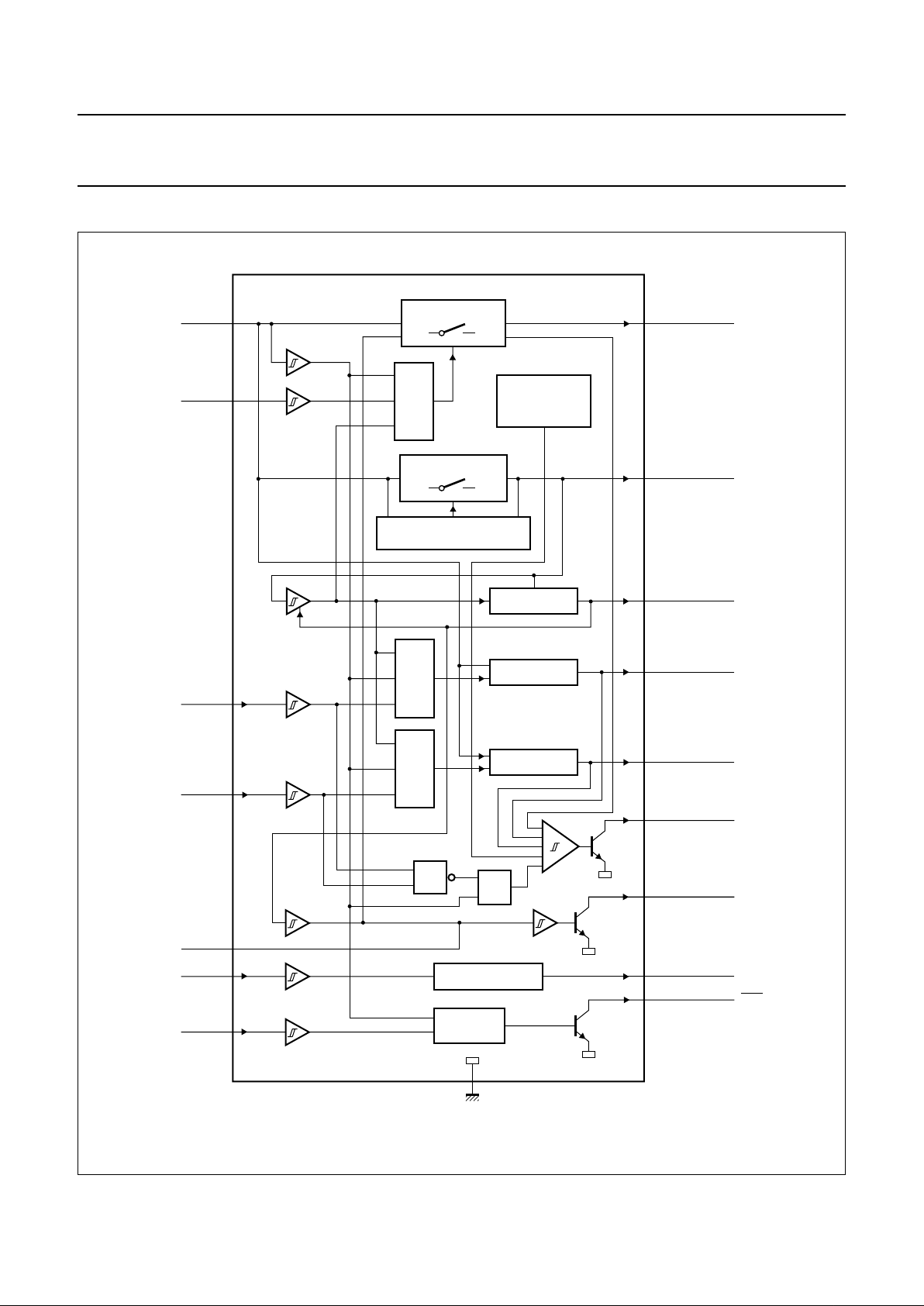
BLOCK DIAGRAM
handbook, full pagewidth
MGR928
REGULATOR 2
REGULATOR 3
REGULATOR 1
17
16
9
TEMPERATURE
LOAD DUMP
PROTECTION
1
11
4
10
13
14
POWER SWITCH
BACK-UP SWITCH
BACK-UP CONTROL
&
&
&
&
≥1
GND
(14.4 V)
TDA3618JR
RES
REG2
REG3
REG1
(14.2 V/3 A)
(14.2 V/100 mA)
(5 V/150 mA)
(5 V/750 mA)
(9 V/600 mA)
SW
V
P
ENSW
EN3
EN1
C
RES
BU
HOLD
12
2
IGNITION BUFFER
5
IGN2
OUT
IGN2
IN
7
INVERTER
6
IGN1
IN
8
3
15
V
thr
= 7 V, V
thf
= 4.5 V
IGN1
OUT
Fig.1 Block diagram.

1999 Sep 01 5
Philips Semiconductors Preliminary specification
Multiple voltage regulator with switch and
ignition buffers
TDA3618JR
PINNING
SYMBOL PIN DESCRIPTION
V
P
1 supply voltage
REG1 2 regulator 1 output
REG3 3 regulator 3 output
EN3 4 enable input regulator 3
IGN2
IN
5 ignition 2 input
IGN1
IN
6 ignition 1 input
IGN1
OUT
7 ignition 1 output (active LOW)
IGN2
OUT
8 ignition 2 output
RES 9 reset output
EN1 10 enable input regulator 1
ENSW 11 enable input power switch
HOLD 12 hold output (active LOW)
C
RES
13 reset delay capacitor
GND 14 ground
REG2 15 regulator 2 output
BU 16 backup
SW 17 power switch output
Fig.2 Pin configuration.
handbook, halfpage
TDA3618JR
MGR929
V
P
REG1
REG3
EN3
IGN2
IN
IGN1
IN
IGN1
OUT
IGN2
OUT
RES
EN1
ENSW
HOLD
C
RES
GND
REG2
BU
SW
1
2
3
4
5
6
7
8
9
10
11
12
13
14
15
16
17

1999 Sep 01 6
Philips Semiconductors Preliminary specification
Multiple voltage regulator with switch and
ignition buffers
TDA3618JR
FUNCTIONAL DESCRIPTION
TheTDA3618JR is a multiple outputvoltage regulator with
a power switch, intended for use in car radios with or
without a microcontroller. Because of the low-voltage
operation of the car radio, low-voltage drop regulators are
used in the TDA3618JR.
Regulator 2 switches on when the backup voltage
exceeds 6.5 V for the first time and switches off again
when the output voltage of regulator 2 falls below 1.9 V
(this is far below an engine start). When regulator 2 is
switched on and its output voltage is within its voltage
range, the reset output is enabled (RES goes HIGH
through a pull-up resistor) to generate a reset to the
microcontroller. The reset cycles can be extended by an
external capacitor at pin 13. This start-up feature is
included to secure a smooth start-up of themicrocontroller
at first connection, without uncontrolled switching of
regulator 2 during the start-up sequence.
The charge of the backup capacitor can be used to supply
regulator 2 for a short period when the supply drops to 0 V
(the time depends on the value of the storage capacitor).
The output stages (regulators 1 and 3) of this regulator
have an extremely low noise behaviour and good stability.
Regulators 1 and 3 are stabilized by using small output
capacitors.
Whenboth regulator 2 and the supply voltage (VP> 4.5 V)
are available, regulators 1 and 3 can be operated by
means of enable inputs (pins 10 and 4 respectively).
TheHOLD output pin isnormally HIGH and is activeLOW.
The HOLD output pin is connected to an open collector
NPN transistor and must have an external pull-up resistor
to operate. The HOLD output is controlled by a LOW
detection circuit which, when activated, pulls the warning
output LOW (enabled). The hold outputs of the regulators
are connected to an OR gate inside the IC such that the
hold is activated (goes LOW) when the regulator voltages
of regulator 1 and/or regulator 3 are out of regulation for
any reason. Each regulator enable input controls its own
hold circuit, such that if a regulator is disabled or switched
off, the hold circuit for that regulator is disabled.
The hold is also controlled by the temperature and load
dump protection. Activating the temperature or load dump
protection causes a hold (LOW) during the time the
protection is activated. When all regulators are switched
off, the HOLD output is controlled by the battery line
(pin 1), temperature protection and load dump protection.
The hold is enabled (LOW) at low battery voltages. This
indicates that it is not possible to get regulator 1 into
regulation when switching it on. The hold function includes
hysteresis to avoid oscillations when the regulator voltage
crosses the hold threshold. The HOLD output becomes
alsoactive(LOW)whentheswitchisinfoldbackprotection
mode, see Fig.4 for a timing diagram. The block diagram
is given in Fig.3.
The power switch can also be controlled by means of a
separate enable input (pin 11).
All output pins are fully protected. The regulators are
protectedagainst load dump (regulators 1 and 3 switch off
at supply voltages >18 V) and short circuit (foldback
current protection).
The switch contains a current protection. However, this
protection is delayed at short circuit by the reset delay
capacitor. During this time, the output current is limited to
a peak value of at least 3 and 2 A continuous (VP≤ 18 V).
In the normal situation, the voltage on the reset delay
capacitor is about 3.5 V (depending on the temperature).
The switch output is about VP− 0.4 V. At operational
temperature, the switch can deliver at least 3 A. At high
temperature, the switch can deliver about 2 A. During an
overload condition or short circuit (VSW<VP−3.7 V), the
voltage on the reset delay capacitor rises 0.6 V above the
voltage of regulator 2. This rise time depends on the
capacitorconnectedontheC
RES
(pin 13).Duringthistime,
the switch can deliver more than 3 A. The charge current
of the reset delay capacitor is typically 4 µA and the
voltage swing about 1.5 V. When regulator 2 is out of
regulation and generates a reset, the switch can only
deliver 2 A and will go in the foldback protection without
delay. At supply voltages >17 V, the switch is clamped at
16 V maximum (to avoid externally connected circuits
being damaged by an overvoltage) and the switch will
switch off at load dump.
Interfacing with the microcontroller (simple full/semi on/off
logic applications) can be realized with two independent
ignition Schmitt triggers and ignition output buffers (one
open collector and one push-pull output). Ignition 1 output
is inverted.
The total timing diagrams are shown in Figs 4 and 5.
1999 Sep 01 7
Philips Semiconductors Preliminary specification
Multiple voltage regulator with switch and
ignition buffers
TDA3618JR
handbook, full pagewidth
&
OR
OR
REGULATOR 1
low battery
detector
internal
voltage ref. 1
internal
voltage
ref. 2
enable
output stage
output stage
enable
out of
regulation
detector
out of
regulation
detector
REGULATOR 3
TDA3618JR
TEMPERATURE
PROTECTION
>150 °C
LOADDUMP
buffer
MGL792
V16
FOLDBACK
MODE
1
10
EN1
REG1
REG3
HOLD
V
P
EN3
4
12
3
2
Fig.3 Block diagram of the HOLD.
1999 Sep 01 8
Philips Semiconductors Preliminary specification
Multiple voltage regulator with switch and
ignition buffers
TDA3618JR
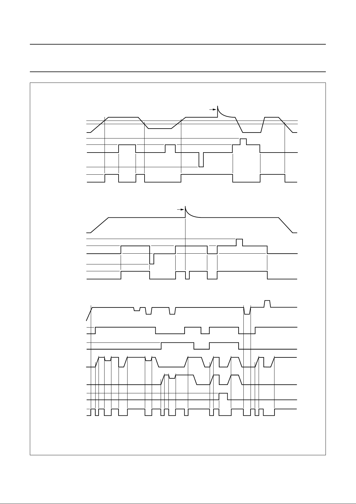
handbook, full pagewidth
load dump
load dump
V
P
ignition 1
input
ignition 1
output
V
P
ignition 2
input
ignition 2
output
7.0 V
4.5 V
≥3.25 V
≥−100 V
5.0 V
≤50 V
≤1.1 V
≥2.2 V
≥−100 V
5.0 V
≤50 V
≤2.0 V
Enable Schmitt trigger ignition 1
Enable Schmitt trigger ignition 2
V
P
enable
regulator 3
enable
regulator 1
regulator 3
regulator 1
temperature
protection
150 °C
HOLD
>1.8 V
>1.3 V
LOW
HIGH
passive
active
>1.8 V
>1.3 V
MGR930
Fig.4 Timing diagram of ignition Schmitt triggers and HOLD.
 Loading...