

Philips TDA3617J-N1 Datasheet

DATA SH EET
Preliminary specification
File under Integrated Circuits, IC01
1999 Jul 14
INTEGRATED CIRCUITS
TDA3617
Multiple voltage regulator
1999 Jul 14 2
Philips Semiconductors Preliminary specification
Multiple voltage regulator TDA3617
FEATURES
General
• Three VP-state controlled regulators
(regulators 1, 2 and 3)
• Very good stability and noise behaviour
• Separate controlpins for switching regulators 1, 2 and 3
• Supply voltage range from −18 to +50 V
• Low quiescent current (when regulators 1, 2 and 3 are
switched off)
• High ripple rejection
• Hold output for indicating regulator 1 and/or 2 and/or 3
out of regulation.
Protections
• Reverse polarity safe (down to −18 V without high
reverse current)
• Able to withstand voltages up to 18 V at the outputs
(supply line may be short circuited)
• ESD protection on all pins
• Thermal protection
• Load dump protection
• Foldback current limit protection for
regulators 1, 2 and 3
• DC short-circuit safe to ground and VP for all regulator
outputs.
GENERAL DESCRIPTION
The TDA3617J is a multiple output voltage regulator with
three independent regulators. It contains:
1. Three fixed voltage regulators with foldback current
protection (regulators 1, 2 and 3)
2. A supply pin that can withstand load dump pulses and
negative supply voltages
3. Independent enable inputs for regulators 1, 2 and 3
4. Local temperature protection for regulator 3
5. A hold output that can be used to interface with a
microprocessor. The hold indicates that the selected
output voltages are available and within their ranges.
QUICK REFERENCE DATA
ORDERING INFORMATION
SYMBOL PARAMETER CONDITIONS MIN. TYP. MAX. UNIT
Supply
V
P
supply voltage
operating 9.5 14.4 17.5 V
jump start t ≤ 10 minutes −−30 V
load dump protection for 50 ms; t
r
≥ 2.5 ms −−50 V
I
q(tot)
total quiescent current standby mode − 540µA
T
j
junction temperature −−175 °C
Voltage regulators
V
REG1
output voltage regulator 1 1 mA ≤ I
REG1
≤ 1.3 A 8.55 9.0 9.45 V
V
REG2
output voltage regulator 2 1 mA ≤ I
REG2
≤ 600 mA;
VP= 14.4 V
4.75 5.0 5.25 V
V
REG3
output voltage regulator 3 1 mA ≤ I
REG3
≤ 300 mA 3.14 3.3 3.46 V
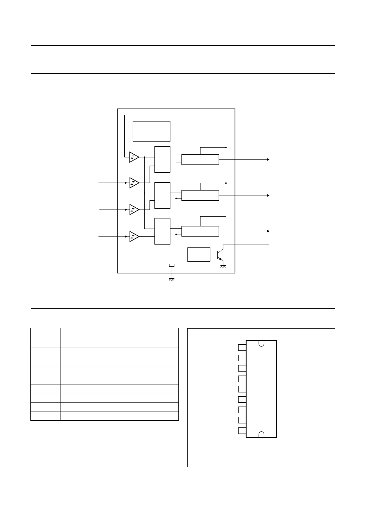
TYPE
NUMBER
PACKAGE
NAME DESCRIPTION VERSION
TDA3617J DBS9P plastic DIL-bent-SIL power package; 9 leads (lead length 7.7 mm) SOT157-4
1999 Jul 14 3
Philips Semiconductors Preliminary specification
Multiple voltage regulator TDA3617
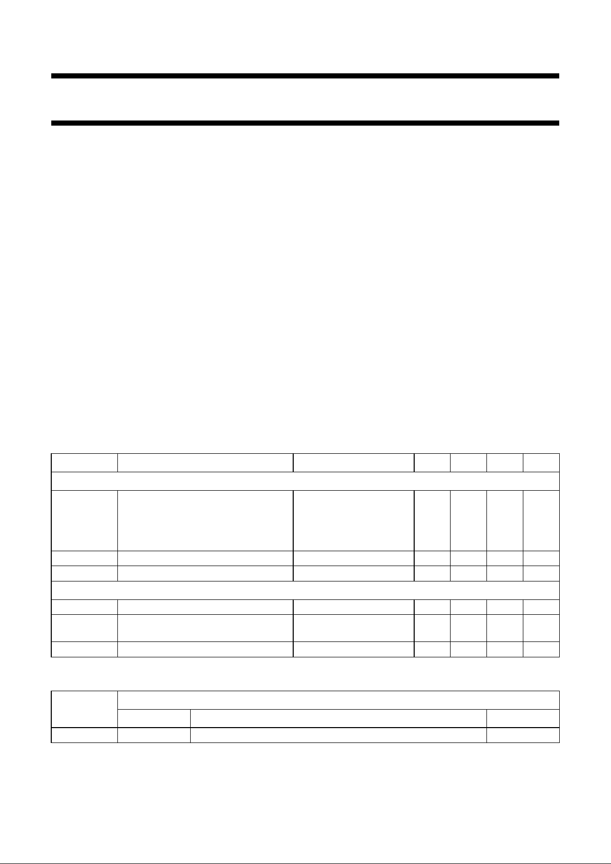
BLOCK DIAGRAM
handbook, full pagewidth
MGL589
TEMPERATURE
LOAD DUMP
PROTECTION
8
GND
(14.4 V)
TDA3617
REG1
REG2
REG3
(9 V/1.3 A)
(5 V/600 mA)
V
P
6
(3.3 V/300 mA)
5
7
4
REGULATOR 2
REGULATOR 3
HOLD
HOLD
1
&
&
REGULATOR 1
&
V
en3
9
V
en2
2
3
V
en1
Fig.1 Block diagram.
PINNING
SYMBOL PIN DESCRIPTION
V
en3
1 enable input regulator 3
V
en1
2 enable input regulator 1
V
P
3 supply voltage
REG1 4 regulator 1 output
REG3 5 regulator 3 output
REG2 6 regulator 2 output
HOLD 7 hold output
GND 8 ground
V
en2
9 enable input regulator 2
Fig.2 Pin configuration.
handbook, halfpage
TDA3617
MGL590
1
2
3
4
5
6
7
8
9
V
en3
V
en1
V
en2
V
P
REG1
REG3
REG2
HOLD
GND
1999 Jul 14 4
Philips Semiconductors Preliminary specification
Multiple voltage regulator TDA3617
FUNCTIONAL DESCRIPTION
The TDA3617J is a multiple output voltage regulator with
threeindependent switchable regulators. Whenthesupply
voltage(VP> 4.5 V)is available, regulators 1, 2 and 3 can
be operated by means of three independentenable inputs.
Schmitt trigger functions are included to switch the
regulators off at low battery voltage (VP< 4 V).
A hysteresis is included to avoid random switching.
All output pins are fully protected. The regulators are
protected against load dump (the regulators switch off at
supply voltages higher than 20 V) and short circuit
(foldback current protection).
The TDA3617J has a hold circuit which indicates when
oneofthe regulators is out-of-regulation. The holdfunction
is disabled when all the enable inputs are LOW
(TDA3617J in standby mode). The HOLD output (open
collector output) can be wired OR-ed with other hold
outputs of other regulator parts (e.g. TDA3618). When all
the regulators of the TDA3617J are disabled (switched
off), the HOLD output will be high ohmic. Because of this
feature, the hold will not influence the hold information
when wired OR-ed with other regulator parts.
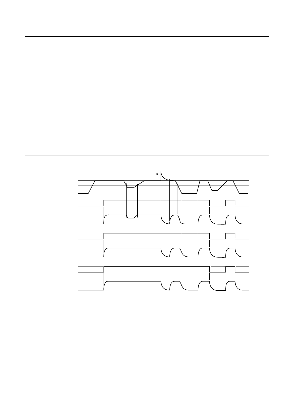
Figure 3 shows the total timing of a semi-on/off logic set.
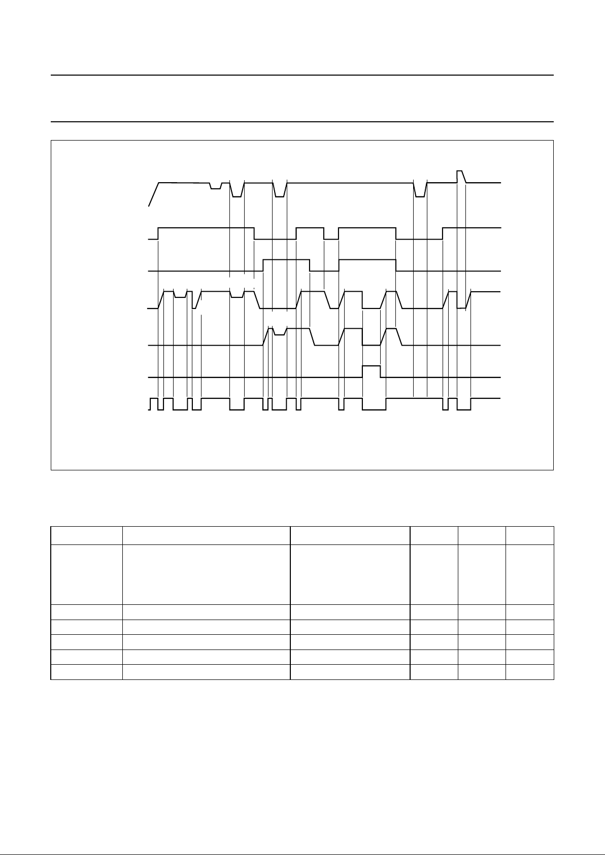
Figure 4 shows the total timing of the HOLD signal.
handbook, full pagewidth
V
P
enable
regulator 1
regulator 1
regulator 2
enable
regulator 2
18.0 V
9.4 V
4.5 V
4.0 V
≥2.2 V
9.0 V
0 V
load dump
5.0 V
0 V
≤2.0 V
≥2.2 V
≤2.0 V
regulator 3
enable
regulator 3
3.3 V
0 V
≥2.2 V
≤2.0 V
MGL621
Fig.3 Timing diagrams of a semi-on/off logic set.
1999 Jul 14 5
Philips Semiconductors Preliminary specification
Multiple voltage regulator TDA3617
LIMITING VALUES
In accordance with the Absolute Maximum Rating System (IEC 134).
SYMBOL PARAMETER CONDITIONS MIN. MAX. UNIT
V
P
supply voltage
operating − 17.5 V
jump start t ≤ 10 minutes − 30 V
load dump protection for 50 ms; t
r
≥ 2.5 ms − 50 V
V
bat(rp)
reverse polarity battery voltage non-operating −−18 V
P
tot
total power dissipation − 62 W
T
stg
storage temperature non-operating −55 +150 °C
T
amb
ambient temperature operating −40 +85 °C
T
j
junction temperature operating − 175 °C
Fig.4 Timing diagrams of the HOLD signal.
handbook, full pagewidth
load dump
V
P
enable
regulator
2 and/or 3
enable
regulator 1
out of
regulation
regulator
output
2 and/or 3
regulator
output 1
temperature
protection
>150 °C
HOLD
passive
active
MGL622
out of
regulation
short
circuit
out of
regulation
 Loading...