


INTEGRATED CIRCUITS
DATA SH EET
TDA3616
Multiple voltage regulator with
battery detection
Product specification
Supersedes data of 2000 Jan 14
File under Integrated Circuits, IC01
2001 Feb 02
Philips Semiconductors Product specification
Multiple voltage regulator with battery
detection
FEATURES
General
• One VP-state controlled regulator
• Battery detection circuit
• Regulator,resetandbatteryoutputsoperateduringload
dump
• Supply voltage range from −18 to +50 V
• Low quiescent current (battery detection switched off)
• High ripple rejection
• Dual reset output
• Backup circuit
• Adjustable reset delay timer.
Protections
• Reverse polarity safe (down to −18 V without high
reverse current)
• Able to withstand voltages up to 18 V at the output
(supply line may be short-circuited)
• ESD protected on all pins
• Load dump protection
• Foldback current limit protection for regulator
• TheregulatoroutputisDCshort-circuitedsafetoground
and VP.
TDA3616
GENERAL DESCRIPTION
The TDA3616 is a low power voltage regulator. It contains
the following:
• One fixed voltage regulator with a foldback current
protection, intended to supply a microprocessor, that
also operates during load dump
• Aprovision for use of a reserve supply capacitor that will
hold enough energy for the regulator to allow a
microcontroller to prepare for loss of supply voltage
• Reset signals which can be used to interface with the
microprocessor
• A supply pin that can withstand load dump pulses and
negative supply voltages
• Definedstart-upbehaviour;regulatorwillbeswitchedon
at a supply voltage higher than 7.5 V and off when the
output voltage of the regulator drops below 2.4 V.
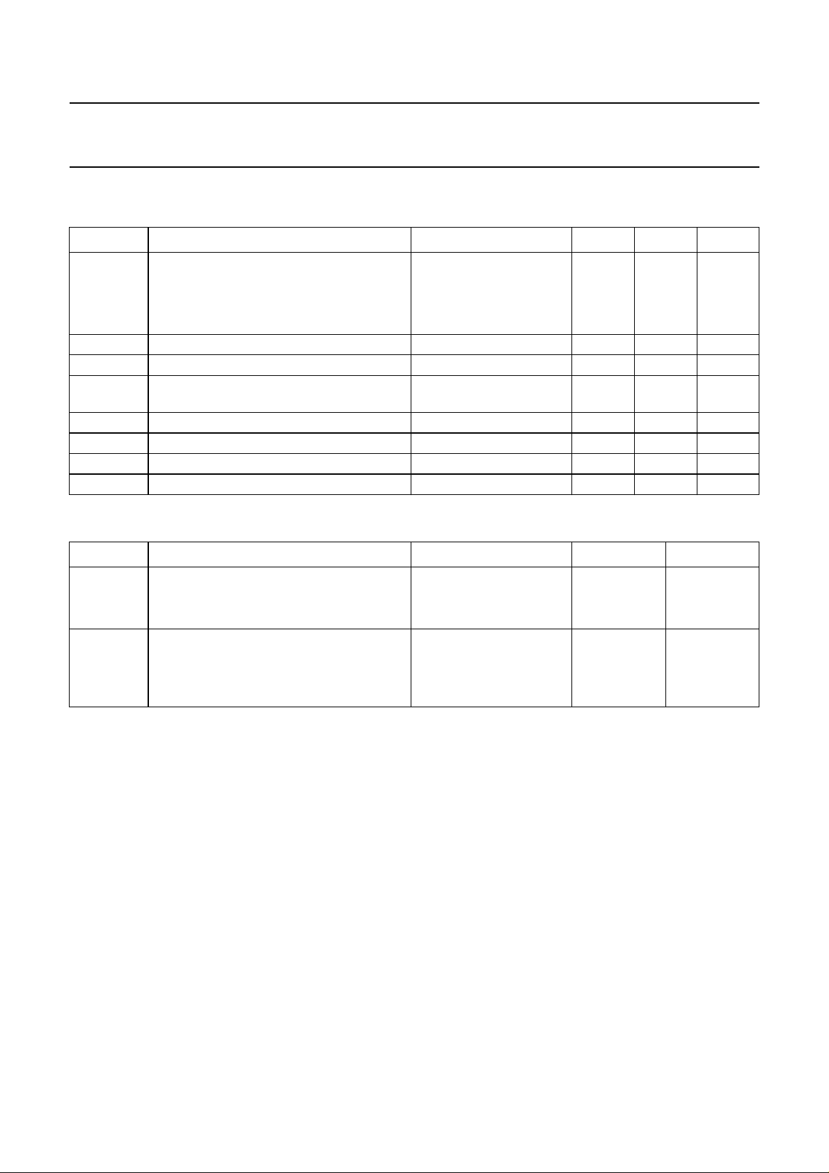
QUICK REFERENCE DATA
SYMBOL PARAMETER CONDITIONS MIN. TYP. MAX. UNIT
Supply
V
P
supply voltage
operating regulator on 5.6 14.4 25 V
jump start t ≤ 10 minutes −−30 V
load dump protection t ≤ 50 ms; t
I
q
quiescent supply current standby mode − 95 125 µA
standby mode; T
≥ 2.5 ms −−50 V
r
=25°C − 95 120 µA
amb
Regulator
V
o
output voltage 0.5 mA ≤ I
7V≤VP≤18 V; T
0.5 mA ≤ I
REG
REG
≤ 150 mA;
=25°C
amb
≤ 150 mA;
4.8 5.0 5.2 V
4.75 5.0 5.25 V
7V≤VP≤18 V
I
REG
= 30 mA;
4.75 5.0 5.25 V
18 V ≤ VP≤ 50 V; load dump
V
drop
drop-out voltage I
= 150 mA; VP=5V;
REG
T
=25°C
amb
− 0.6 1.0 V
2001 Feb 02 2
Philips Semiconductors Product specification
Multiple voltage regulator with battery
TDA3616
detection
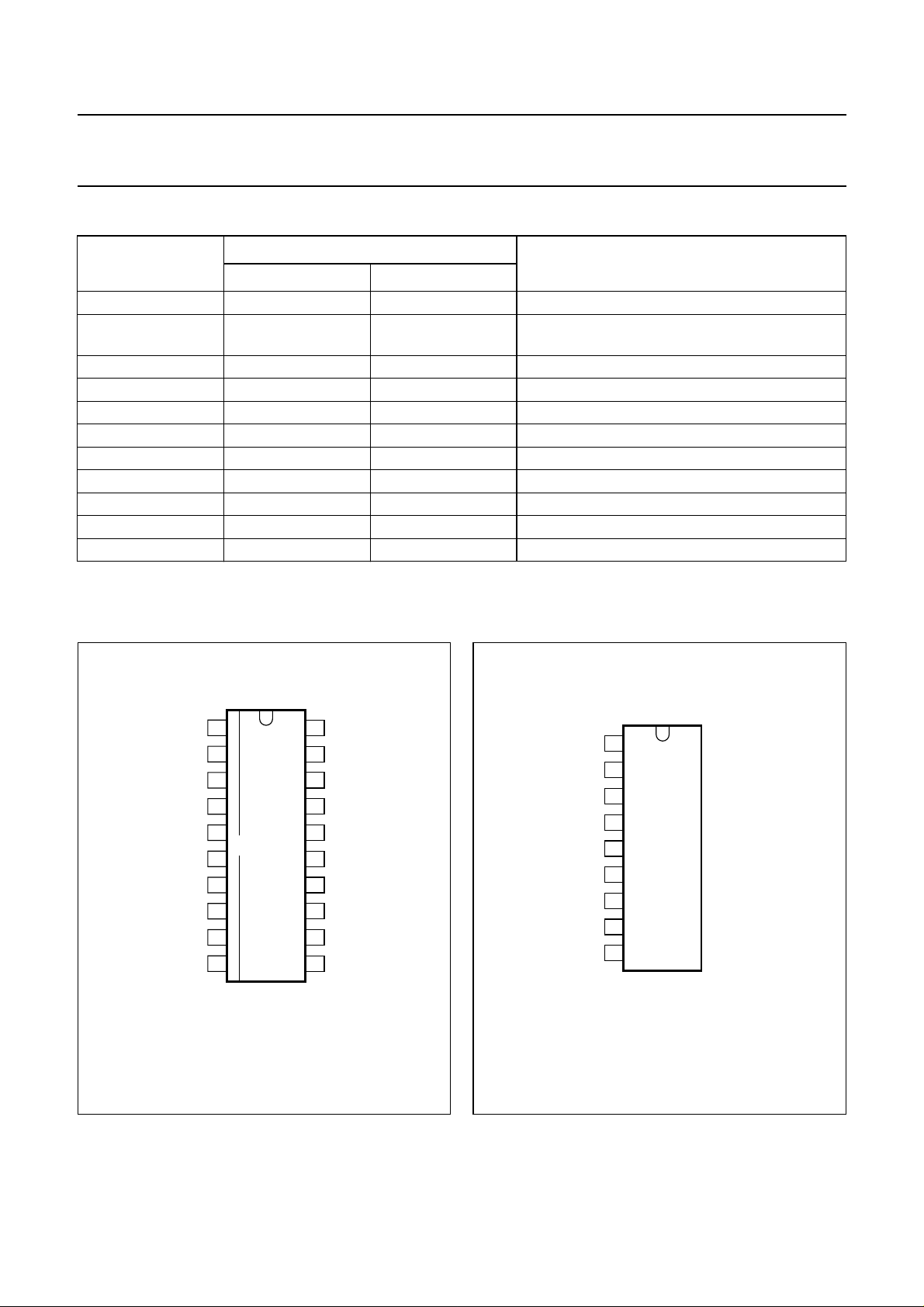
ORDERING INFORMATION
TYPE
NUMBER
NAME DESCRIPTION VERSION
TDA3616T SO20 plastic small outline package; 20 leads; body width 7.5 mm SOT163-1
TDA3616SF SIL9MP plastic single in-line medium power package with fin; 9 leads SOT110-1
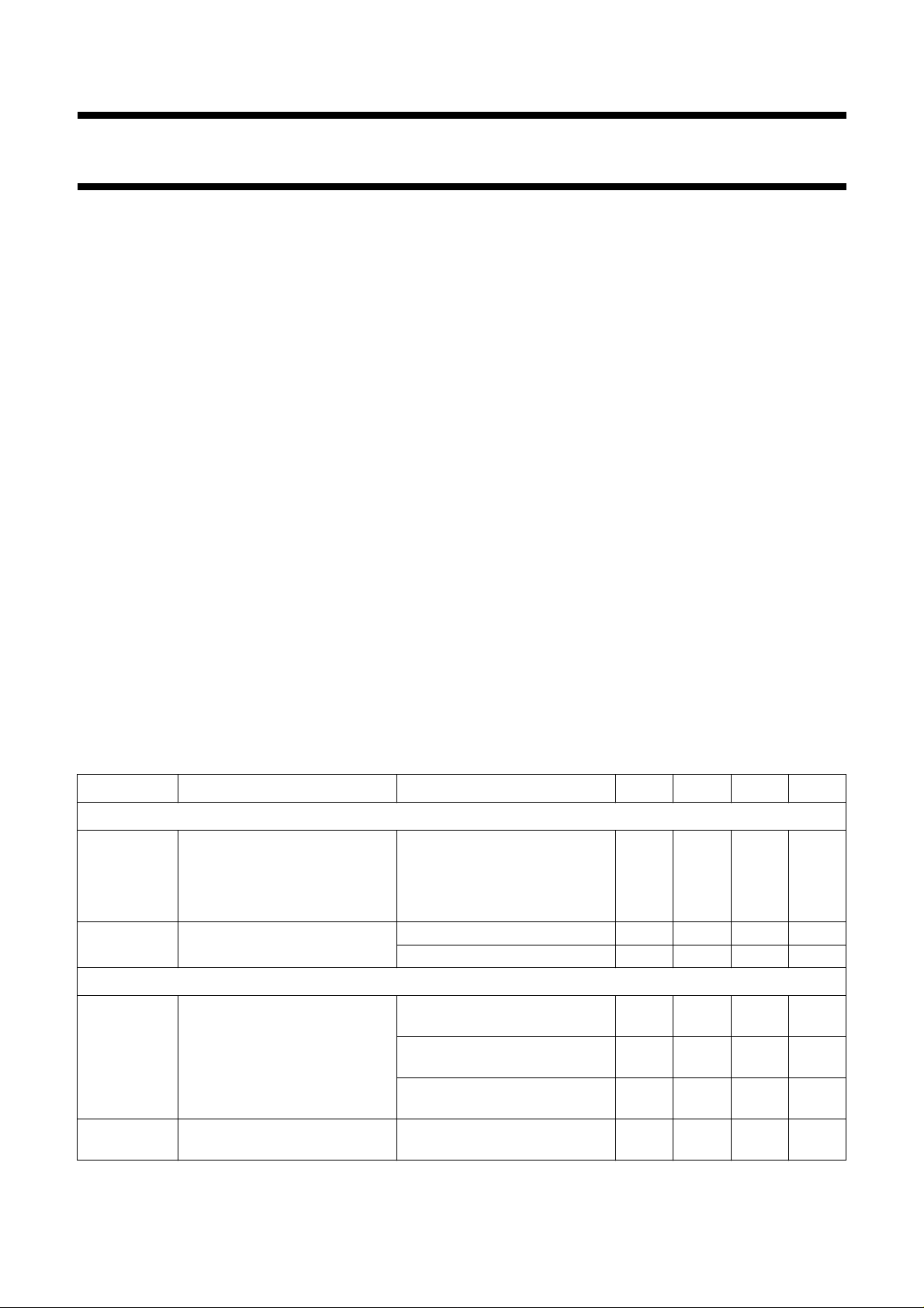
BLOCK DIAGRAM
handbook, full pagewidth
V
(14.4 V)
P
17 (4)
BACKUP SWITCH
PACKAGE
(5) 18
BU
V
n.c.
i.c.
V
I(bat)
3.1
kΩ
3.1
kΩ
(3) 16
(1) 14
(2) 15
(7) 54 (6)
MGL933
REG
RES2
RES1
V
O(bat)
LOAD DUMP
PROTECTION
REFERENCE
2, 3, 8, 9,
12, 13, 19
7
1, 10,
11, 20
4
6 (8)
C
47 kΩ
TDA3616T
7 (9)
GND
REG
BATTERY
BUFFER
REGULATOR
&
The pin numbers given in parenthesis refer to the TDA3616SF version.
Fig.1 Block diagram.
2001 Feb 02 3
Philips Semiconductors Product specification
Multiple voltage regulator with battery
TDA3616
detection
PINNING
SYMBOL
SOT163-1 SOT110-1
i.c. 1, 10, 11, and 20 − interconnected; heat spreader; note 1
n.c. 2, 3, 8, 9, 12, 13
and 19
V
I(bat)
V
O(bat)
V
C
4 6 battery input voltage
5 7 battery detection output voltage
6 8 reset delay capacitor
GND 7 9 ground (0 V)
RES2 14 1 reset 2 output
RES1 15 2 reset 1 output
REG 16 3 regulator output
V
P
17 4 supply voltage
BU 18 5 backup
Note
1. The i.c. pins are connected to each other by the leadframe and can be kept floating or can be connected to ground.
PIN
DESCRIPTION
− not connected; heat spreader
handbook, halfpage
The i.c. and n.c. pins can be connected to a heat spreader.
V
V
O(bat)
i.c.
n.c.
n.c.
I(bat)
V
GND
n.c.
n.c.
i.c.
C
1
2
3
4
5
TDA3616T
6
7
8
9
10
MGR093
i.c.
20
19
n.c.
18
BU
V
17
P
16
REG
RES1
15
RES2
14
n.c.
13
n.c.
12
i.c.
11
Fig.2 Pin configuration (SOT163-1).
handbook, halfpage
Fig.3 Pin configuration (SOT110-1).
RES2
RES1
V
V
O(bat)
REG
V
BU
I(bat)
V
GND
1
2
3
4
P
5
6
7
8
C
9
TDA3616SF
MGL930
2001 Feb 02 4
Philips Semiconductors Product specification
Multiple voltage regulator with battery
detection
FUNCTIONAL DESCRIPTION
The TDA3616 (see Fig.1) is a voltage regulator intended
to supply a microprocessor (e.g. in car radio applications).
Because of low-voltage operation of the application, a
low-voltage drop regulator is used.
This regulator will switch-on when the backup voltage
(see Section “Backup circuit”) exceeds 7.5 V for the first
time and will switch-off again when the output voltage of
the regulator drops below 2.4 V. When the regulator is
switched on, the RES1 and RES2 outputs (RES2 can only
be HIGH when RES1 is HIGH) will go HIGH after a fixed
delay time (fixed by an external delay capacitor) to
generate a reset to the microprocessor.
Pin RES1 will go HIGH via an internal pull-up resistor of
3.1 kΩ, and is used to initialize the microprocessor.
Pin RES2 is used to indicate that the regulator output
voltage is within its voltage range. This start-up feature is
built-in to secure a smooth start-up of the microprocessor
at first connection, without uncontrolled switching of the
regulator during the start-up sequence.
TDA3616
The charge of the backup capacitor can be used to supply
the regulator and logic circuits for a short period of time
whenthesupplyfallsto0 V (the time depends on the value
of the storage capacitor). The regulator is switched off at a
backup voltage of approximately 2.7 V. From this time
onwards, the backup charge will only be used for
maintaining reset functions. Due to this, the reset outputs
willremainLOWuntiltheoutputoftheregulatoris dropped
to 0 V.
All output pins are fully protected. The regulator is
protected against load dump and short-circuit (foldback
current protection). At load dump, the battery detection
circuit will remain operating.
Interfacing with the microprocessor can be accomplished
by means of a battery Schmitt trigger and output buffer
(simple full/semi on/off logic applications). The battery
output will go HIGH when the battery input voltage
exceeds the high threshold level.
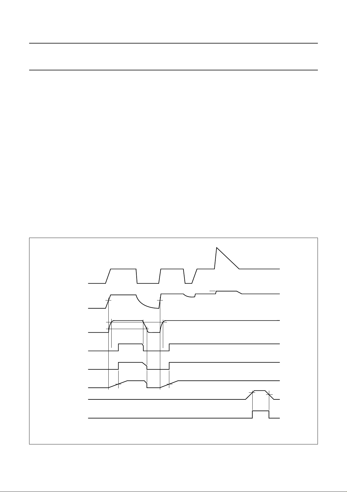
The timing diagrams are shown in Fig.4.
handbook, full pagewidth
reset delay
battery input
battery output
V
V
BU
regulator
reset 2
reset 1
capacitor
P
18 V
4.75 V
2.4 V
2 V2 V
2.05 V
1.95 V
MGR095
Fig.4 Timing diagrams.
2001 Feb 02 5
Philips Semiconductors Product specification
Multiple voltage regulator with battery
TDA3616
detection
LIMITING VALUES
In accordance with the Absolute Maximum Rating System (IEC 134).
SYMBOL PARAMETER CONDITIONS MIN. MAX. UNIT
V
P
V
rp
V
I(bat)p
V
I(bat)n
P
tot
T
stg
T
amb
T
j
THERMAL CHARACTERISTICS
supply voltage
operating regulator on − 25 V
jump start t ≤ 10 minutes − 30 V
load dump protection t ≤ 50 ms; t
≥ 2.5 ms − 50 V
r
reverse polarity voltage non-operating −−18 V
positive pulse voltage at battery input VP= 14.4 V; RI=5kΩ− 50 V
negative pulse voltage at battery input VP= 14.4 V; RI=10kΩ;
−−100 V
Cl=1nF
total power dissipation VP= 12.4 V − 2.5 W
storage temperature non-operating −55 +150 °C
ambient temperature operating −40 +105 °C
junction temperature operating −40 +150 °C
SYMBOL PARAMETER CONDITIONS VALUE UNIT
R
th(j-p)
thermal resistance from junction to pin/tab
TDA3616T 20 K/W
TDA3616SF 12 K/W
R
th(j-a)
thermal resistance from junction to ambient
TDA3616T 10 cm
2
2-sided copper
50 K/W
area connected to pins
TDA3616SF in free air 50 K/W
QUALITY SPECIFICATION
Quality specification in accordance with
“SNW-FQ-611E”
.
2001 Feb 02 6
 Loading...