

Philips tda3608q th DATASHEETS

INTEGRATED CIRCUITS
DATA SH EET
TDA3608Q; TDA3608TH
Multiple voltage regulators with
switch
Product specification
Supersedes data of 1997 Aug 14
File under Integrated Circuits, IC01
2000 Oct 13

Philips Semiconductors Product specification
Multiple voltage regulators with switch TDA3608Q; TDA3608TH
FEATURES
General
• Two VP-state controlled regulators (regulator 1 and
regulator 3) and a power switch
• Regulator 2 and reset circuit operate during load dump
and thermal shutdown
• Separate control pins for switching regulator 1,
regulator 3 and power switch
• Supply voltage range from −18 to +50 V
• Low reverse current of regulator 2
• Low quiescent current (when regulator 1, regulator 3
and power switch are switched off)
• Hold output circuit for regulator 1 (only valid when
regulator 3 output voltage >1.3 V)
• Reset and hold outputs (open-collector outputs)
• Adjustable reset delay time
• High ripple rejection
• Backup capacitor connection to supply regulator 2 and
reset circuit up to 25 V.
Protections
• Reverse polarity safe (down to −18 V without high
reverse current)
• Able to withstand voltages up to 18 V at the outputs
(supply line may be short circuited)
• ESD protection on all pins
• Thermal protection
• Load dump protection
• Foldback current limit protection for regulator 1,
regulator 2 and regulator 3
• Delayed foldback current limit protection for power
switch (at short-circuit); delay time fixed by reset delay
capacitor
• All regulator outputs and power switch are
DC short-circuited safe to ground and VP.
GENERAL DESCRIPTION
The TDA3608 isamultiple output voltage regulator with a
power switch, intended for use in car radios with or without
a microcontroller. It contains:
• Two fixed output voltage regulators with a foldback
current protection (regulator 1 and regulator 3) and one
fixed output voltage regulator (regulator 2) intended to
supply a microcontroller, which also operates during
load dump and thermal shutdown
• A power switch with protections, operated by an enable
input
• Reset and hold outputs that can be used to interface
with the microcontroller; the reset output can be used to
call up the microcontroller and the hold output indicates
thattheregulator 1 output voltage is available and within
the range
• A supply pin which can withstand load dump pulses and
negative supply voltages
• Regulator 2 which is switched on at a backup voltage
higher than 6.5 V and switched off when the regulator 2
output drops below 1.9 V
• A provision for the use of a reserve (backup) supply
capacitor that will hold enough energy for regulator 2
(5 Vcontinuous) to allow a microcontrollertoprepare for
loss of voltage.
2000 Oct 13 2

Philips Semiconductors Product specification
Multiple voltage regulators with switch TDA3608Q; TDA3608TH
QUICK REFERENCE DATA
SYMBOL PARAMETER CONDITIONS MIN. TYP. MAX. UNIT
Supply
V
P
I
q
T
j
Voltage regulators
V
REG1
V
REG2
V
REG3
Power switch
V
drop
I
M
supply voltage operating 9.5 14.4 18 V
regulator 2 on 2.4 14.4 18 V
reverse polarity; non-operating −−−18 V
jump start for t ≤ 10 minutes −−30 V
load dump protection for t ≤ 50 ms
and t
≥ 2.5 ms
r
−−50 V
quiescent supply current standby mode; VP= 12.4 V − 500 600 µA
junction temperature −40 − +150 °C
output voltage of regulator 1 1 mA ≤ I
output voltage of regulator 2 0.5 mA ≤ I
output voltage of regulator 3 1 mA ≤ I
≤ 600 mA 8.15 8.5 8.85 V
REG1
≤ 150 mA 4.75 5.0 5.25 V
REG2
≤ 400 mA 4.75 5.0 5.25 V
REG3
dropout voltage ISW=1A − 0.45 0.7 V
I
= 1.8 A − 1.0 1.8 V
SW
peak current 2 −−A
ORDERING INFORMATION
TYPE
NUMBER
NAME DESCRIPTION VERSION
PACKAGE
TDA3608Q DBS13P plastic DIL-bent-SIL power package; 13 leads (lead length 12 mm) SOT141-6
TDA3608TH HSOP20 plastic, heatsink small outline package; 20 leads; low stand-off height SOT418-2
2000 Oct 13 3
Philips Semiconductors Product specification
Multiple voltage regulators with switch TDA3608Q; TDA3608TH
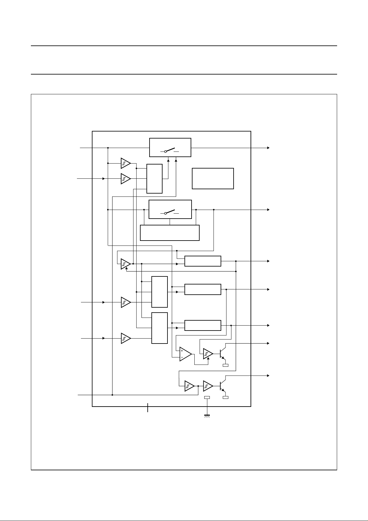
BLOCK DIAGRAM
handbook, full pagewidth
(14.4 V)
V
1 (3)
P
POWER SWITCH
(17) 13
SW
(14.2 V/1.8 A)
ENSW
EN3
EN1
7 (10)
4 (6)
6 (9)
&
BACKUP SWITCH
BACKUP CONTROL
&
&
TEMPERATURE
AND LOAD DUMP
PROTECTION
REGULATOR 2
REGULATOR 3
REGULATOR 1
(16) 12
(15) 11
(5) 3
(4) 2
(11) 8
BU
REG2
REG3
REG1
HOLD
(14.2 V/100 mA)
(5 V/150 mA)
(5 V/400 mA)
(8.5 V/600 mA)
TDA3608Q
hold enable
(TDA3608TH)
C
9 (12)
RES
(1, 2, 7, 13, 18, 19, 20)
n.c.
Numbers in parenthesis refer to type number TDA3608TH.
Fig.1 Block diagram.
2000 Oct 13 4
10 (14)
GND
(8) 5
MGK602
RES

Philips Semiconductors Product specification
Multiple voltage regulators with switch TDA3608Q; TDA3608TH
PINNING
SYMBOL
DESCRIPTION
TDA3608Q TDA3608TH
PIN
V
P
1 3 supply voltage
REG1 2 4 regulator 1 output
REG3 3 5 regulator 3 output
EN3 4 6 regulator 3 enable input
RES 5 8 reset output
EN1 6 9 regulator 1 enable input
ENSW 7 10 power switch enable input
HOLD 8 11 hold output
C
RES
9 12 reset delay capacitor connection
GND 10 14 ground
REG2 11 15 regulator 2 output
BU 12 16 backup capacitor connection
SW 13 17 power switch output
n.c. − 1, 2, 7, 13, 18,
not connected
19 and 20
handbook, halfpage
Fig.2 Pin configuration of TDA3608Q.
V
REG1
REG3
EN3
RES
EN1
ENSW
HOLD
C
RES
GND
REG2
BU
SW
P
1
2
3
4
5
6
TDA3608Q
7
8
9
10
11
12
13
MGK601
handbook, halfpage
Fig.3 Pin configuration of TDA3608TH.
n.c.
n.c.
V
REG1
REG3
EN3
n.c.
RES
EN1
ENSW
1
2
3
P
4
5
6
7
8
9
10
TDA3608TH
MGT566
n.c.
20
n.c.
19
n.c.
18
17
SW
16
BU
REG2
15
GND
14
n.c.
13
C
12
RES
HOLD
11
2000 Oct 13 5

Philips Semiconductors Product specification
Multiple voltage regulators with switch TDA3608Q; TDA3608TH
FUNCTIONAL DESCRIPTION
The TDA3608 is a multiple output voltage regulator with a
power switch, intended for use in car radios with or without
a microcontroller. Because of low-voltage operation of the
car radio, low-voltage drop regulators are used in the
TDA3608.
Backup supply
The charge of the backup capacitor connected to pin BU
can be used to supply regulator 2 for a short period when
the supply voltage VP drops to 0 V (the time depends on
the value of the capacitor).
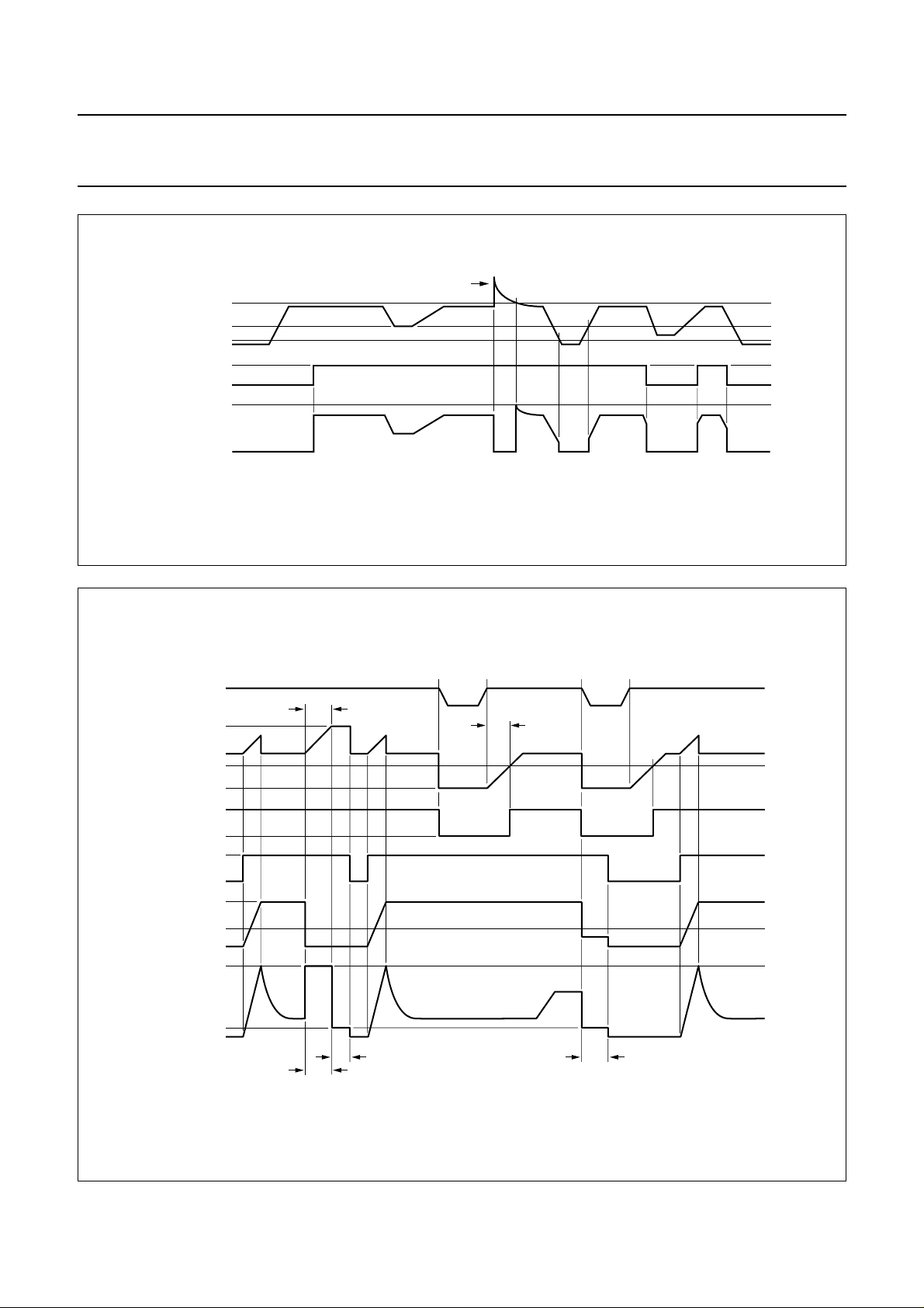
Regulator 1
When the output voltage of regulator 2 and the supply
voltage (VP> 4.5 V) are both available, regulator 1 can be
operated by means of enable pin EN1 (see Fig.4).
Regulator 2
Regulator 2 switches on (see Fig.5) when the backup
voltage exceeds 6.5 V for the first time and switches off
when the output voltage of regulator 2 drops below 1.9 V
(this is far below an engine start).
The hold output is only activated when V
REG3
> 1.3 V.
When pin HOLD is connected via a pull-up resistor to the
output of regulator 3 spikes will be minimized to 1.3 V
(maximum value) because the hold output is only disabled
when V
REG3
< 1.3 V.
Pin HOLD will be forced LOW when the load dump
protection is activated and also in the standby mode.
Power switch
The power switch can be controlled by means of enable
pin ENSW (see Fig.6).
Protections
All output pins are fully protected.
The regulators are protected against load dump
(regulator 1 and regulator 3 switch off at VP> 18 V) and
short-circuit (foldback current protection).
The power switch contains a foldback current protection,
but this protection is delayed at a short-circuit condition by
the reset delay capacitor. During this time the output
current is limited to at least 2 A (peak value) and
1.8 A (continuous value) at VP≤ 18 V. During the foldback
mode the current is limited to 0.5 A (typical value).
Regulator 3
When the output voltage of regulator 2 and the supply
voltage (VP> 4.5 V) are both available, regulator 3 can be
operated by means of enable pin EN3 (see Fig.4).
Reset
When regulator 2 is switched on and the output voltage of
this regulator is within its voltage range, the reset output
(see Fig.5) will be enabled (pin RES goes HIGH through
an external pull-up resistor) to generate a reset to the
microcontroller.
The reset cycles can be extended by means of anexternal
capacitor connected to pin C
. This start-up feature is
RES
included to secure asmooth start-up ofthe microcontroller
at first connection, without uncontrolled switching of
regulator 2 during the start-up sequence.
Hold
Regulator 1 has an open-collector hold output (see Fig.4)
indicating that the output voltage is settled at 8.5 V.
Pin HOLD is held HIGH by an external pull-up resistor.
When the supply voltage VPdrops or during high load, the
output voltage drops out-of-regulationand pin HOLD goes
LOW.
The timing diagram is shown in Fig.7.
The foldback protection is activated when VSW<4V.
When regulator 2 is out-of-regulation and generates a
reset, the power switch is in the foldback mode
immediately when VSW<4V.
In the standby mode the voltage on the reset delay
capacitor is about 4 V and the voltage on the power switch
output is VP− 0.45 V (typical value) at ISW= 1 A. During
an overload condition or short-circuit the reset delay
capacitor will be charged to a higher voltage. The power
switch is in the high current mode while the capacitor is
charged, after this the switch is in the foldback mode
(VSW< 4 V).Whilethe reset delay capacitor is charged the
power switch output can reach its correct output voltage.
Now the voltage on the reset delay capacitor is decreased
rapidlyto 4 V. The resetoutput voltage is not influencedby
this change of voltages. The time of the high current mode
depends on the value of the reset delay capacitor.
At VP> 18 V the power switch is clamped at maximum
17.2 V (to avoid that external connected circuitry is being
damaged by an overvoltage) and the power switch will
switch off at load dump.
2000 Oct 13 6

Philips Semiconductors Product specification
Multiple voltage regulators with switch TDA3608Q; TDA3608TH
handbook, full pagewidth
V
P
enable
regulator 1
regulator 1
enable
regulator 3
regulator 3
hold output
18.0 V
9.5 V
4.5 V
4.0 V
≥2.2 V
≤2.0 V
8.5 V
0 V
≥2.2 V
≤2.0 V
5.0 V
load dump
0 V
MGT568
Fig.4 Timing diagram of regulator 1, regulator 3 and hold output.
handbook, full pagewidth
V
P
backup
regulator 2
reset
delay
capacitor
reset
output
18.0 V
4.0 V
6.5 V
5.4 V
5.0 V
1.9 V
0 V
5.0 V
3.0 V
0 V
5.0 V
t
d(res)
load dump
Fig.5 Timing diagram of backup, regulator 2 and reset output.
2000 Oct 13 7
MGT567
Philips Semiconductors Product specification
Multiple voltage regulators with switch TDA3608Q; TDA3608TH
handbook, full pagewidth
V
P
enable
power
switch
power
switch
output
handbook, full pagewidth
regulator 2
reset
delay
voltage
reset
output
enable
power
switch
power
switch
voltage
power
switch
current
18.0 V
4.5 V
4.0 V
≥2.2 V
≤2.0 V
16.2 V
0 V
5 V
6.4 V
4 V
3 V
0 V
5 V
0 V
>
2.2 V
<
2.0 V
14 V
4 V
0 V
2 A
0.5 A
0 A
current limit mode
load dump
Fig.6 Timing diagram of power switch output.
t
d(sw)
foldback mode foldback mode
t
d(res)
MGT569
MGT570
Fig.7 Timing diagram of current protection of power switch.
2000 Oct 13 8
 Loading...