

Philips tda3607 DATASHEETS

INTEGRATED CIRCUITS
DATA SH EET
TDA3607
Multiple voltage regulator with
switch
Preliminary specification
File under Integrated Circuits, IC01
1997 May 05
Philips Semiconductors Preliminary specification
Multiple voltage regulator with switch TDA3607
FEATURES
• Three VP-state controlled regulators (regulator 1,
regulator 2 and regulator 3)
• Separate control pins for switching regulators 1, 2 and 3
• Supply voltage range from −18 to +50 V
• Low quiescent current (when regulators 1, 2 and 3 are
switched off)
• High ripple rejection.
PROTECTIONS
• Reverse polarity safe (down to −18 V without high
reverse current)
• Able to withstand voltages up to 18 V at the outputs
(supply line may be short-circuited)
• ESD protected on all pins
• Thermal protection
• Load dump protection
• Foldback current limit protection for
regulators 1, 2 and 3
• DC short-circuit safe to ground and V
for all regulator
P
outputs.
GENERAL DESCRIPTION
The TDA3607 is a multiple output voltage regulator with
three independent regulators. It contains:
1. Three fixed voltage regulators with foldback current
protection (regulators 1, 2 and 3)
2. A supply pin which can withstand load dump pulses
and negative supply voltages
3. Independant enable inputs for regulators 1, 2 and 3
4. Local temperature protection for regulator 3.
QUICK REFERENCE DATA
SYMBOL PARAMETER CONDITIONS MIN. TYP. MAX. UNIT
Supply
V
P
supply voltage
operating 11 14.4 18 V
jump start t ≤ 10 minutes −−30 V
≥ 2.5 ms −−50 V
r
I
q(tot)
T
j
load dump protection during 50 ms; t
total quiescent current standby mode − 140µA
junction temperature −−150 °C
Voltage regulators
V
V
REG1
REG2
output voltage regulator 1 0.5 mA ≤ I
output voltage regulator 2 0.5 mA ≤ I
≤ 1.3 A 8.55 9.0 9.45 V
REG1
REG2
≤ 150 mA;
4.75 5.0 5.25 V
VP= 14.4 V
V
REG3
output voltage regulator 3 0.5 mA ≤ I
≤ 400 mA 4.75 5.0 5.25 V
REG3
ORDERING INFORMATION
TYPE
NUMBER
NAME DESCRIPTION VERSION
TDA3607 SIL9P
plastic single in-line power package; 9 leads
PACKAGE
SOT131-2
1997 May 05 2
Philips Semiconductors Preliminary specification
Multiple voltage regulator with switch TDA3607
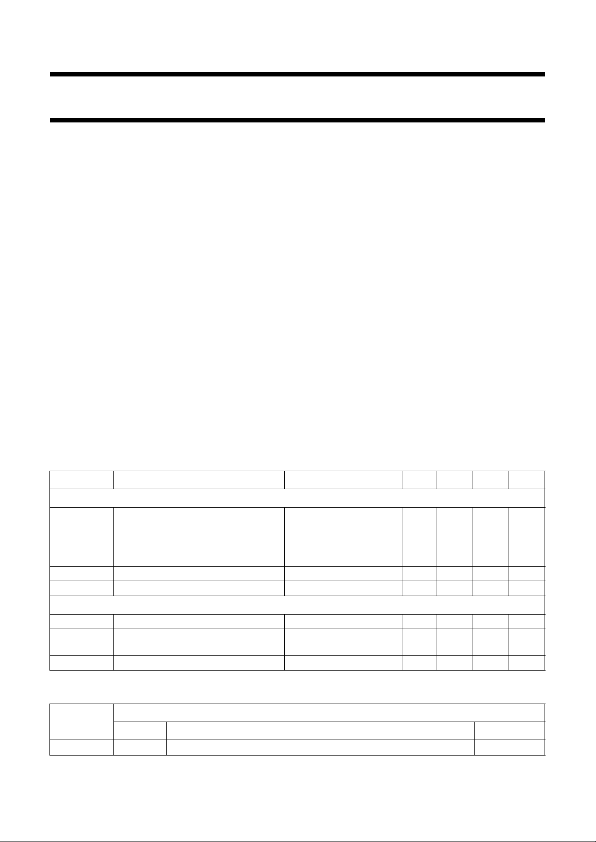
BLOCK DIAGRAM
handbook, full pagewidth
V
DEC
V
en1
V
en2
V
en3
(14.4 V)
P
3
7
2
9
1
TEMPERATURE
LOAD DUMP
PROTECTION
&
&
&
REGULATOR 1
REGULATOR 2
REGULATOR 3
8
GND
TDA3607
MBG718
4
(9 V/1.3 A)
(5 V/150 mA)
6
(5 V/400 mA)
5
REG1
REG2
REG3
Fig.1 Block diagram.
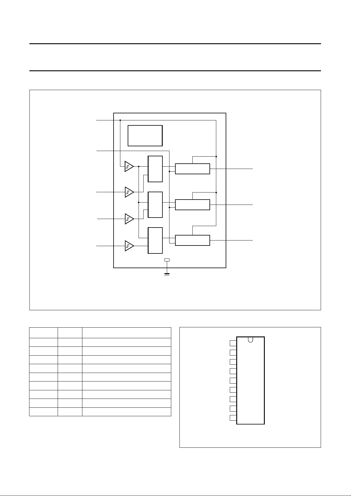
PINNING
SYMBOL PIN DESCRIPTION
V
en3
V
en1
V
P
1 enable input regulator 3
2 enable input regulator 1
3 supply voltage
REG1 4 regulator 1 output
REG3 5 regulator 3 output
REG2 6 regulator 2 output
DEC 7 decoupling capacitor
GND 8 ground
V
en2
9 enable input regulator 2
1997 May 05 3
handbook, halfpage
1
V
en3
2
V
en1
3
V
P
4
REG1
5
REG3
REG2
DEC
GND
V
en2
TDA3607
6
7
8
9
MBG717
Fig.2 Pin configuration.

Philips Semiconductors Preliminary specification
Multiple voltage regulator with switch TDA3607
FUNCTIONAL DESCRIPTION
The TDA3607 is a multiple output voltage regulator with
three independent switchable regulators. When the supply
voltage (VP> 4.5 V) is available, regulators 1, 2 and 3 can
be operated by means of 3 independent enable inputs.
Schmitt-trigger functions are included to switch-off the
regulators at low battery voltage (VP< 4 V). A hysteresis is
included to avoid random switching.
handbook, full pagewidth
V
enable
regulator 1
regulator 1
enable
regulator 2
regulator 2
enable
regulator 3
regulator 3
18.0 V
9.4 V
P
4.5 V
4.0 V
≥2.2 V
≤2.0 V
9.0 V
0 V
≥2.2 V
≤2.0 V
5.0 V
0 V
≥2.2 V
≤2.0 V
5.0 V
0 V
load dump
All output pins are fully protected. The regulators are
protected against load dump (regulators will switch-off at
supply voltages higher than 20 V) and short-circuit
(foldback current protection).
The total timing of a semi on/off logic set is shown in Fig.3.
MBG720
Fig.3 Timing diagrams.
1997 May 05 4

Philips Semiconductors Preliminary specification
Multiple voltage regulator with switch TDA3607
LIMITING VALUES
SYMBOL PARAMETER CONDITIONS MIN. MAX. UNIT
V
P
V
P
P
tot
T
stg
T
amb
T
j
THERMAL CHARACTERISTICS
SYMBOL PARAMETER CONDITIONS VALUE UNIT
R
th j-c
R
th j-a
supply voltage
operating − 18 V
jump start t ≤ 10 minutes − 30 V
load dump protection during 50 ms; t
≥ 2.5 ms − 50 V
r
reverse battery voltage non-operating −−18 V
total power dissipation − 62 W
storage temperature range non-operating −55 +150 °C
ambient temperature range operating −40 +85 °C
junction temperature operating − 150 °C
thermal resistance from junction to case regulator and switch-on 2 K/W
thermal resistance from junction to ambient in free air 50 K/W
QUALITY SPECIFICATION
In accordance with
Handbook”
. The handbook can be ordered using the code 9397 750 00192.
“SNW-FQ-611-E”
. The number of the quality specification can be found in the
“Quality Reference
CHARACTERISTICS
= 14.4 V; T
V
P
=25°C; measured in test circuit of Fig.5; unless otherwise specified.
amb
SYMBOL PARAMETER CONDITIONS MIN. TYP. MAX. UNIT
Supplies
V
P
supply voltage
operating 11 14.4 18 V
REGn on note 1 6 14.4 18 V
jump start t ≤ 10 minutes −−30 V
load dump protection during 50 ms; t
I
q
quiescent current VP= 12.4 V; note 2 − 140µA
= 14.4 V; note 2 − 1 −µA
V
P
≥ 2.5 ms −−50 V
r
Schmitt-trigger power supply for regulators 1, 2 and 3
V
thr
V
thf
V
hys
rising voltage threshold Ven=3V − 4.5 − V
falling voltage threshold Ven=3V − 4.1 − V
hysteresis − 0.4 − V
1997 May 05 5
 Loading...