

Philips TDA3606AT-N1 Datasheet

DATA SH EET
Product specification
Supersedes data of 1997 Aug 12
File under Integrated Circuits, IC01
1998 May 07
INTEGRATED CIRCUITS
TDA3606A
Multiple voltage regulator with
battery detection

1998 May 07 2
Philips Semiconductors Product specification
Multiple voltage regulator with battery
detection
TDA3606A
FEATURES
• One VP-state controlled regulator
• Regulator and reset outputs operate during load dump
• Supply voltage range of −18 to +50 V
• Low quiescent current (battery detection switched off)
• High ripple rejection
• Dual reset output.
PROTECTIONS
• Reverse polarity safe (down to −18 V without high
reverse current)
• Able to withstand voltages up to 18 V at the output
(supply line may be short-circuited)
• ESD protected on all pins
• Load dump protection
• Foldback current limit protection for regulator
• DC short-circuit safe to ground and V
P
of regulator
output.
GENERAL DESCRIPTION
The TDA3606A is a low power voltage regulator.
It contains:
1. One fixed voltage regulator with a foldback current
protection, intended to supply a microprocessor, that
also operates during load dump
2. A reset-signal can be used to interface with the
microprocessor
3. Supply pin can withstand load dump pulses and
negative supply voltages
4. Defined start-up behaviour; regulator will be switched
on at a supply voltage higher than 7.6 V and off when
the output voltage of the regulator drops below 2.4 V.
QUICK REFERENCE DATA
ORDERING INFORMATION
SYMBOL PARAMETER CONDITIONS MIN. TYP. MAX. UNIT
Supplies
V
P
supply voltage
operating regulator on 5.6 14.4 25 V
jump start t ≤ 10 minutes −−30 V
load dump protection t ≤ 50 ms; t
r
≥ 2.5 ms −−50 V
I
q(tot)
total quiescent supply current standby mode − 95 120 µA
Voltage regulator
V
REG
output voltage regulator 7 V ≤ VP≤ 18 V 4.85 5.0 5.15 V
0.5 mA ≤ I
REG
≤ 150 mA 4.8 5.0 5.2 V
V
REGd
drop-out voltage I
REG
= 150 mA −−0.5 V
TYPE
NUMBER
PACKAGE
NAME DESCRIPTION VERSION
TDA3606AT SO20 plastic small outline package; 20 leads; body width 7.5 mm SOT163-1
1998 May 07 3
Philips Semiconductors Product specification
Multiple voltage regulator with battery
detection
TDA3606A
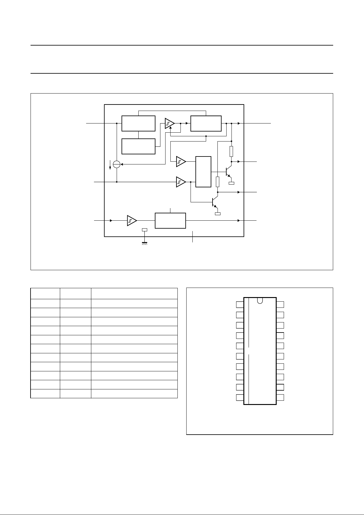
BLOCK DIAGRAM
Fig.1 Block diagram.
handbook, full pagewidth
MGK597
REGULATOR
LOAD DUMP
PROTECTION
REFERENCE
7
&
GND
1 to 3, 8 to 13, 18 to 20
n.c.
TDA3606A
REG
REG
RES2
RES1
(14.4 V)
(5 V/150 mA)
14
16
BATTERY
BUFFER
V
O(bat)
V
I(bat)
V
C
V
P
15
5
4
6
17
4.7
kΩ
4.7
kΩ
PINNING
SYMBOL PIN DESCRIPTION
n.c. 1 to 3 not connected; heat spreader
V
I(bat)
4 battery input voltage
V
O(bat)
5 battery detection output voltage
V
C
6 reset delay capacitor
GND 7 ground (0 V)
n.c. 8 to 13 not connected; heat spreader
RES2 14 reset 2 output
RES1 15 reset 1 output
REG 16 regulator output
V
P
17 supply voltage
n.c. 18 to 20 not connected; heat spreader
Fig.2 Pin configuration.
handbook, halfpage
n.c.
n.c.
n.c.
V
I(bat)
V
O(bat)
V
C
GND
n.c.
n.c.
n.c.
n.c.
n.c.
n.c.
V
P
RES1
RES2
REG
n.c.
n.c.
n.c.
1
2
3
4
5
6
7
8
9
10
11
12
20
19
18
17
16
15
14
13
TDA3606AT
MGK600
1998 May 07 4
Philips Semiconductors Product specification
Multiple voltage regulator with battery
detection
TDA3606A
FUNCTIONAL DESCRIPTION
The TDA3606A is a voltage regulator intended to supply a
microprocessor (e.g. in car radio applications). Because of
low voltage operation of the application, a low-voltage drop
regulator is used in the TDA3606A.
This regulator will switch on when the supply voltage
exceeds 7.6 V for the first time and will switch off again
when the output voltage of the regulator drops below
2.4 V. When the regulator is switched on, the RES1 and
RES2 outputs (RES2 can only be HIGH when RES1 is
HIGH) will go HIGH after a fixed delay time (fixed by an
external delay capacitor) to generate a reset to the
microprocessor.
RES1 will go HIGH by an internal pull-up resistor of 4.7 kΩ,
and is used to initialize the microprocessor. RES2 is used
to indicate that the regulator output voltage is within its
voltage range. This start-up feature is built-in to secure a
smooth start-up of the microprocessor at first connection,
without uncontrolled switching of the regulator during the
start-up sequence.
All output pins are fully protected. The regulator is
protected against load dump and short-circuit (foldback
current protection).
Interfacing with the microprocessor can be accomplished
by means of a battery Schmitt-trigger and output buffer
(simple full/semi on/off logic applications). The battery
output will go HIGH when the battery input voltage
exceeds the HIGH threshold level.
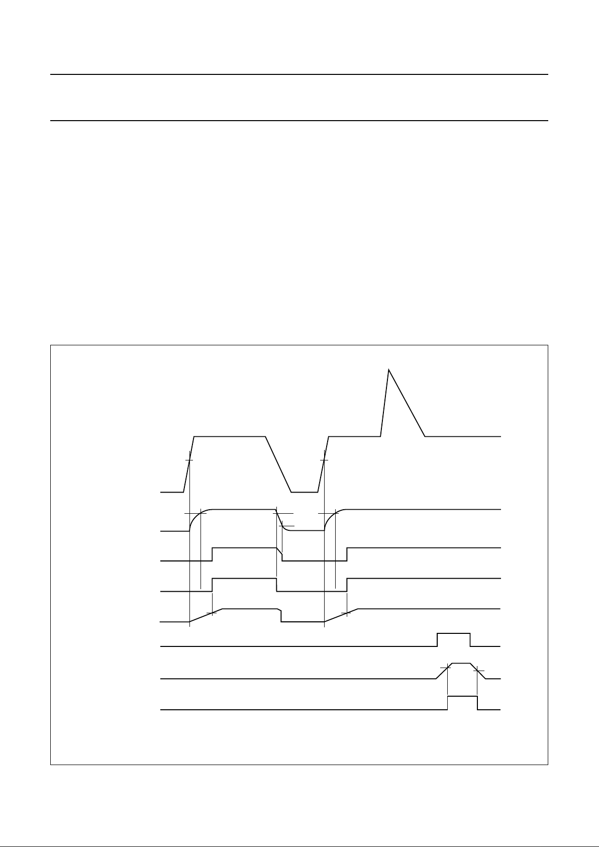
Fig.3 Timing diagrams.
handbook, full pagewidth
2.1 V
V
P
regulator
reset 1
50 V
4.35 V 4.35 V
2.4 V
2 V 2 V
2 V
reset 2
on/off switch
battery input
battery output
reset delay
capacitor
MGB857

1998 May 07 5
Philips Semiconductors Product specification
Multiple voltage regulator with battery
detection
TDA3606A
LIMITING VALUES
In accordance with the Absolute Maximum Rating System (IEC 134).
THERMAL CHARACTERISTICS
Notes
1. On IMS board.
2. On standard board with double sided copper area connected to pins.
QUALITY SPECIFICATION
In accordance with
“SNW-FQ-611E”
. The number of the quality specification can be found in the
“Quality Reference
Handbook”
. The handbook can be ordered using the code 9397 750 00192.
SYMBOL PARAMETER CONDITIONS MIN. MAX. UNIT
V
P
supply voltage
operating regulator on − 25 V
jump start t ≤ 10 minutes − 30 V
load dump protection t ≤ 50 ms; t
r
≥ 2.5 ms − 50 V
V
P
reverse battery voltage non-operating −−18 V
V
I(bat)p
positive pulse voltage at battery input VP= 14.4 V; RI=5kΩ− 50 V
V
I(bat)n
negative pulse voltage at battery input VP= 14.4 V; RI=5kΩ− −100 V
P
tot
total power dissipation T
amb
=25°C − 2.5 W
T
stg
storage temperature non-operating −55 +150 °C
T
amb
operating ambient temperature −40 +85 °C
T
j
junction temperature operating −40 +150 °C
SYMBOL PARAMETER CONDITIONS VALUE UNIT
R
th (j-p)
thermal resistance from junction to pins 20 K/W
R
th (j-a)
thermal resistance from junction to
ambient
in free air; note 1 50 K/W
in free air; note 2 60 K/W
 Loading...