

Philips TDA3605Q-N2, TDA3605Q-N3, TDA3605Q-N1-S420, TDA3605Q-N1 Datasheet

DATA SH EET
Preliminary specification
Supersedes data of 1995 Nov 20
File under Integrated Circuits, IC01
1997 Jul 09
INTEGRATED CIRCUITS
TDA3605Q
Multiple voltage regulator with
switch

1997 Jul 09 2
Philips Semiconductors Preliminary specification
Multiple voltage regulator with switch TDA3605Q
FEATURES
• Two VP-state controlled regulators (regulator 1 and
regulator 3) and a power switch
• Regulator 2, reset and ignition buffer operates during
load dump and thermal shutdown
• Separate control pins for switching regulator 1,
regulator 3 and the power switch
• Supply voltage range of −18 to +50 V (operating from
11 V)
• Low reverse current of regulator 2
• Low quiescent current (when regulator 1, regulator 3,
and power switch are switched off)
• Hold output (only valid when regulator 1 is switched on)
• Reset and hold outputs (open collector outputs)
• Adjustable reset delay time
• High ripple rejection
• Back-up capacitor for regulator 2.
PROTECTIONS
• Reverse polarity safe (down to −18 V without high
reverse current)
• Able to withstand voltages up to 18 V at the outputs
(supply line may be short-circuited)
• ESD protected on all pins
• Thermal protection
• Local thermal protection for power switch
• Load dump protection
• Foldback current limit protection for
regulators 1, 2 and 3
• Delayed second current limit protection for the power
switch (at short-circuit)
• The regulator outputs and the power switch are DC
short-circuited safe to ground and V
P
.
GENERAL DESCRIPTION
The TDA3605Q is a multiple output voltage regulator with
a power switch, intended for use in car radios with or
without a microcontroller. It contains:
1. Two fixed voltage regulators with a foldback current
protection (regulator 1 and regulator 3) and one fixed
voltage regulator (regulator 2), intended to supply a
microcontroller, that also operates during load dump
and thermal shutdown.
2. A power switch with protections, operated by an
enable input.
3. Reset and hold outputs can be used to interface by the
microcontroller. The reset signal can be used to call up
the microcontroller and the hold output indicates
regulator 1 voltage available and within range.
4. A supply pin which can withstand load dump pulses
and negative supply voltage.
5. Regulator 2 will be switched on at a supply voltage
>6.5 V and off at a voltage of regulator 2 <1.9 V.
6. Also there is a provision for use of a reserve supply
capacitor that will hold enough energy for regulator 2
(5 V continuous) to allow a microcontroller to prepare
for loss of voltage.
ORDERING INFORMATION
TYPE NUMBER
PACKAGE
NAME DESCRIPTION VERSION
TDA3605Q DBS13P
plastic DIL-bent-SIL power package; 13 leads (lead length 12 mm)
SOT141-6
1997 Jul 09 3
Philips Semiconductors Preliminary specification
Multiple voltage regulator with switch TDA3605Q
QUICK REFERENCE DATA
SYMBOL PARAMETER CONDITIONS MIN. TYP. MAX. UNIT
Supply
V
P
supply voltage
operating 11 14.4 18 V
reverse battery −18 −−V
regulator 2 on 2.4 14.4 18 V
jump start t ≤ 10 minutes −−30 V
load dump protection during ≤50 ms; t
r
≥ 2.5 ms −−50 V
I
q(tot)
total quiescent supply current standby mode − 500 600 µA
T
j
junction temperature −−150 °C
Voltage regulators
V
REG1
output voltage regulator 1 0.5 mA ≤ I
REG1
≤ 600 mA 9.5 10.0 10.5 V
V
REG2
output voltage regulator 2 0.5 mA ≤ I
REG2
≤ 300 mA; VP= 14.4 V 4.75 5.0 5.25 V
V
REG3
output voltage regulator 3 0.5 mA ≤ I
REG3
≤ 400 mA 4.75 5.0 5.25 V
Power switch
V
sw(d)
drop-out voltage Isw=1A − 0.45 0.7 V
I
sw
= 1.8 A − 1 1.8 V
I
swM
peak current 3 −−A
1997 Jul 09 4
Philips Semiconductors Preliminary specification
Multiple voltage regulator with switch TDA3605Q
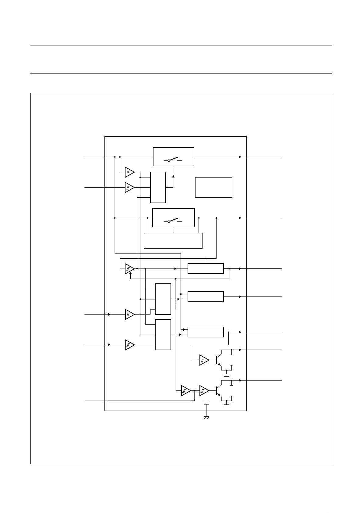
BLOCK DIAGRAM
Fig.1 Block diagram.
handbook, full pagewidth
MGB753
REGULATOR 2
REGULATOR 3
REGULATOR 1
13
12
5
TEMPERATURE
LOAD DUMP
PROTECTION
1
7
4
6
9
10
POWER SWITCH
BACK-UP SWITCH
BACK-UP CONTROL
&
&
&
GND
(14.4 V)
TDA3605Q
RES
REG2
REG3
REG1
(14.2 V/3 A)
(14.2 V/100 mA)
(5 V/100 mA)
(5 V/400 mA)
(10 V/600 mA)
V
sw
V
P
V
en(sw)
V
en3
V
en1
V
C
V
bu
V
hold
1 A after 10 ms
(short-circuit)
8
2
3
11
1997 Jul 09 5
Philips Semiconductors Preliminary specification
Multiple voltage regulator with switch TDA3605Q
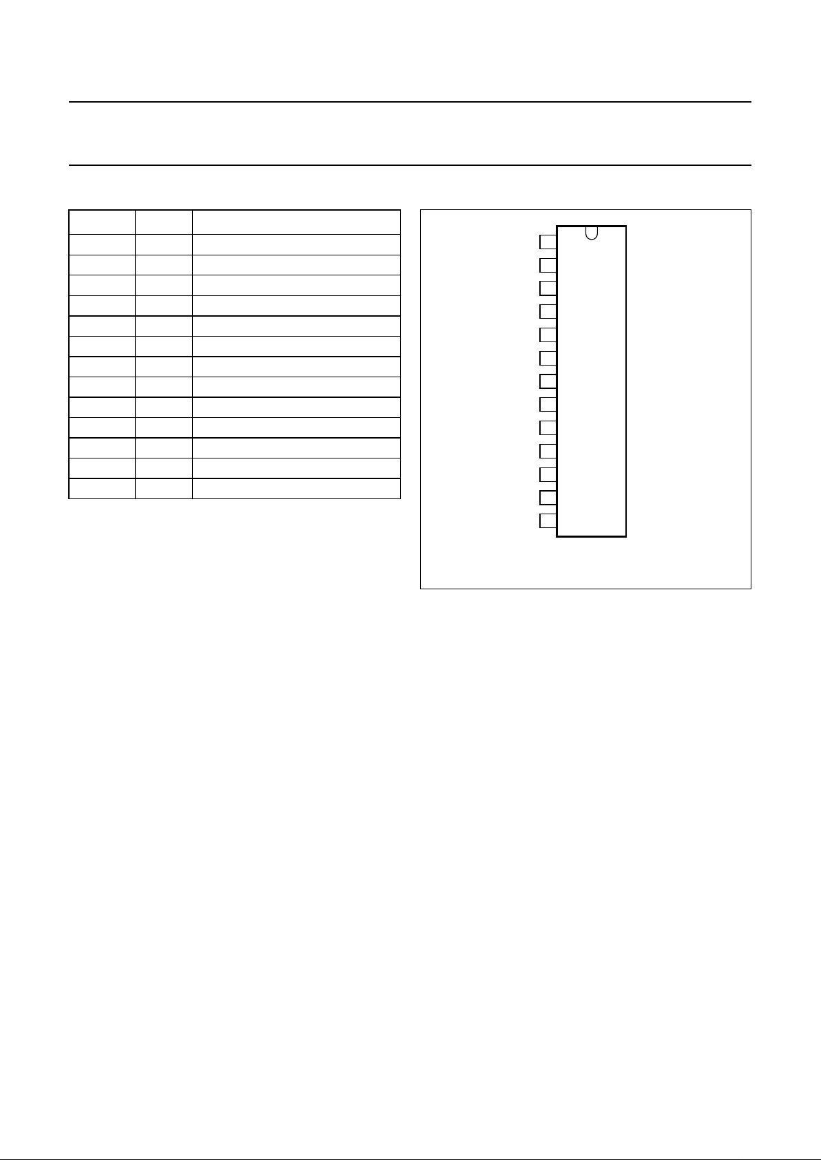
PINNING
SYMBOL PIN DESCRIPTION
V
P
1 supply voltage
REG1 2 regulator 1 output
REG3 3 regulator 3 output
V
en3
4 enable input regulator 3
RES 5 reset output voltage
V
en1
6 enable input regulator 1
V
en(sw)
7 enable input power switch
V
hold
8 hold output
V
C
9 reset delay capacitor
GND 10 ground (0 V)
REG2 11 regulator 2 output
V
bu
12 back-up
V
sw
13 power switch output voltage
Fig.2 Pin configuration.
handbook, halfpage
TDA3605Q
MGB752
1
2
3
4
5
6
7
8
9
10
11
12
13
V
P
REG1
REG3
V
en3
V
en1
V
en(sw)
V
hold
REG2
RES
V
sw
V
bu
V
C
GND
FUNCTIONAL DESCRIPTION
The TDA3605Q is a multiple output voltage regulator with
a power switch, intended for use in car radios with or
without a microcontroller. Because of low-voltage
operation of the car radio, low-voltage drop regulators are
used in the TDA3605Q.
Regulator 2 will switch-on when the back-up voltage
exceeds 6.5 V for the first time and will switch-off again
when the output voltage of regulator 2 is below 1.9 V
(this is far below an engine start). When regulator 2 is
switched on and the output voltage of this regulator is
within its voltage range, the reset output will be enabled
(reset will go HIGH via a pull-up resistor) to generate a
reset to the microcontroller. The reset cycles can be
extended by an external capacitor at pin 9. The above
mentioned start-up feature is built-in to secure a smooth
start-up of the microcontroller at first connection, without
uncontrolled switching of regulator 2 during the start-up
sequence.
The charge of the back-up capacitor can be used to supply
regulator 2 for a short period when the supply falls to 0 V
(time depends on value of storage capacitor). When both
regulator 2 and the supply voltage (V
P
> 4.5 V) are
available, regulators 1 and 3 can be operated by means of
enable inputs (pins 6 and 4 respectively).
Regulator 1 has a hold output (open collector) indicating
that the output voltage of this regulator is settled
(held HIGH by external pull-up resistor) and when the
output voltage of this regulator drops out of regulation
(because of supply voltage drop or high load) the hold
output will go LOW. The hold output signal is only valid
when regulator 1 is enabled by its enable input (pin 6).
The power switch can also be controlled by means of a
separate enable input (pin 7).
All output pins are fully protected. The regulators are
protected against load dump (regulator 1 and 3 will switch
off at supply voltages >18 V) and short-circuit (foldback
current protection).
The switch contains a current protection, but this
protection is delayed at short-circuit condition for at least
10 ms. During this time the output current is limited to a
peak value of at least 3 A and 2 A (DC) (V
P
≤ 18 V).
At supply voltages >17 V the switch is clamped at
maximum 16 V (to avoid external connected circuitry being
damaged by an overvoltage) and the switch will switch-off
at load dump.
The total timing of a semi on/off logic set is shown in Fig.3.
 Loading...