

Philips TDA3604TH-N1-S420, TDA3604TH-N2, TDA3604TH-N1, TDA3604Q-N1 Datasheet

DATA SH EET
Product specification
Supersedes data of 1997 Aug 15
File under Integrated Circuits, IC01
1997 Aug 21
INTEGRATED CIRCUITS
TDA3604Q; TDA3604TH
Multiple voltage regulators with
external reset delay and switch

1997 Aug 21 2
Philips Semiconductors Product specification
Multiple voltage regulators with external
reset delay and switch
TDA3604Q;
TDA3604TH
FEATURES
General
• One V
P
-state controlled regulator (regulator 2)
• Regulator 2, reset and ignition buffer operate during
load dump and thermal shutdown
• Separate control pins for switching regulator 1 and the
power switch
• Supply voltage range of −18 to +50 V
(operating from 9.75 V)
• Low reverse current of regulator 2
• Low quiescent current (when regulator 1, power switch
and ignition buffer are switched off)
• Ignition input/output
• Reset output
• Adjustable reset delay time
• High ripple rejection
• Power switch
• Separate supply for the power switch.
Protections
• Reverse polarity safe (down to −18 V without high
reverse current)
• Able to withstand voltages up to 18 V at the outputs
(supply line may be short-circuited)
• ESD protected on all pins
• Thermal protection
• Load dump protection
• Foldback current limit protection for regulators 1 and 2
• Delayed second current limit protection for the power
switch
• The regulator outputs and the power switch are
DC short-circuited safe to ground and V
P
.
GENERAL DESCRIPTION
The TDA3604Q and TDA3604TH are multiple output
voltage regulators with a power switch, intended for use in
car radios with or without a microcontroller.
It contains one fixed voltage regulator with a foldback
current protection (regulator 1) and one fixed voltage
regulator (regulator 2), intended to supply a
microcontroller, that also operates during load dump and
thermal shutdown.
There is a power switch with protections, operated by an
enable input.
The reset and ignition outputs can be used to interface by
the microcontroller. The reset signal can be used to call up
the microcontroller and the ignition output indicates
ignition voltage available.
Both supply pins can withstand load dump pulses and
negative supply voltages.
Regulator 2 will be switched on at a supply voltage >6.5 V
and off at a voltage of regulator 2 <1.9 V.
ORDERING INFORMATION
TYPE
NUMBER
PACKAGE
NAME DESCRIPTION VERSION
TDA3604Q DBS13P plastic DIL-bent-SIL power package; 13 leads (lead length 12 mm) SOT141-6
TDA3604TH HSOP20 plastic heat-dissipating small outline package; 20 leads; low stand-off SOT418-2
1997 Aug 21 3
Philips Semiconductors Product specification
Multiple voltage regulators with external
reset delay and switch
TDA3604Q; TDA3604TH
QUICK REFERENCE DATA
Notes
1. Minimum operating voltage, only if V
P
has exceeded 6.5 V.
2. The drop-out voltage of regulator 1 is measured between VPand V
REG1
.
3. The drop-out voltage of the power switch is measured between V
I(sw)
and V
O(sw)
.
SYMBOL PARAMETER CONDITIONS MIN. TYP. MAX. UNIT
Supply
V
P
supply voltage
operating 9.75 14.4 25 V
regulator 2 on note 1 2.4 14.4 25 V
jump start t ≤ 10 minutes −−30 V
load dump protection during 50 ms; t
r
≥ 2.5 ms −−50 V
I
q
total quiescent current standby mode − 400 500 µA
T
vj
operating virtual junction
temperature
−−150 °C
Voltage regulators
V
REG1
output voltage regulator 1 0.5 mA ≤ I
REG1
≤ 300 mA 8.65 9.0 9.35 V
V
REG2
output voltage regulator 2 0.5 mA ≤ I
REG2
≤ 50 mA; VP= 14.4 V 4.8 5.0 5.2 V
V
REGd1
drop-out voltage regulator 1 I
REG1
= 0.3 A; note 2 −−0.5 V
Power switch
V
swd
drop-out voltage Isw= 0.5 A; note 3 −−1.4 V
I
swM
peak current t ≤ 10 ms 1.4 −−A
1997 Aug 21 4
Philips Semiconductors Product specification
Multiple voltage regulators with external
reset delay and switch
TDA3604Q; TDA3604TH
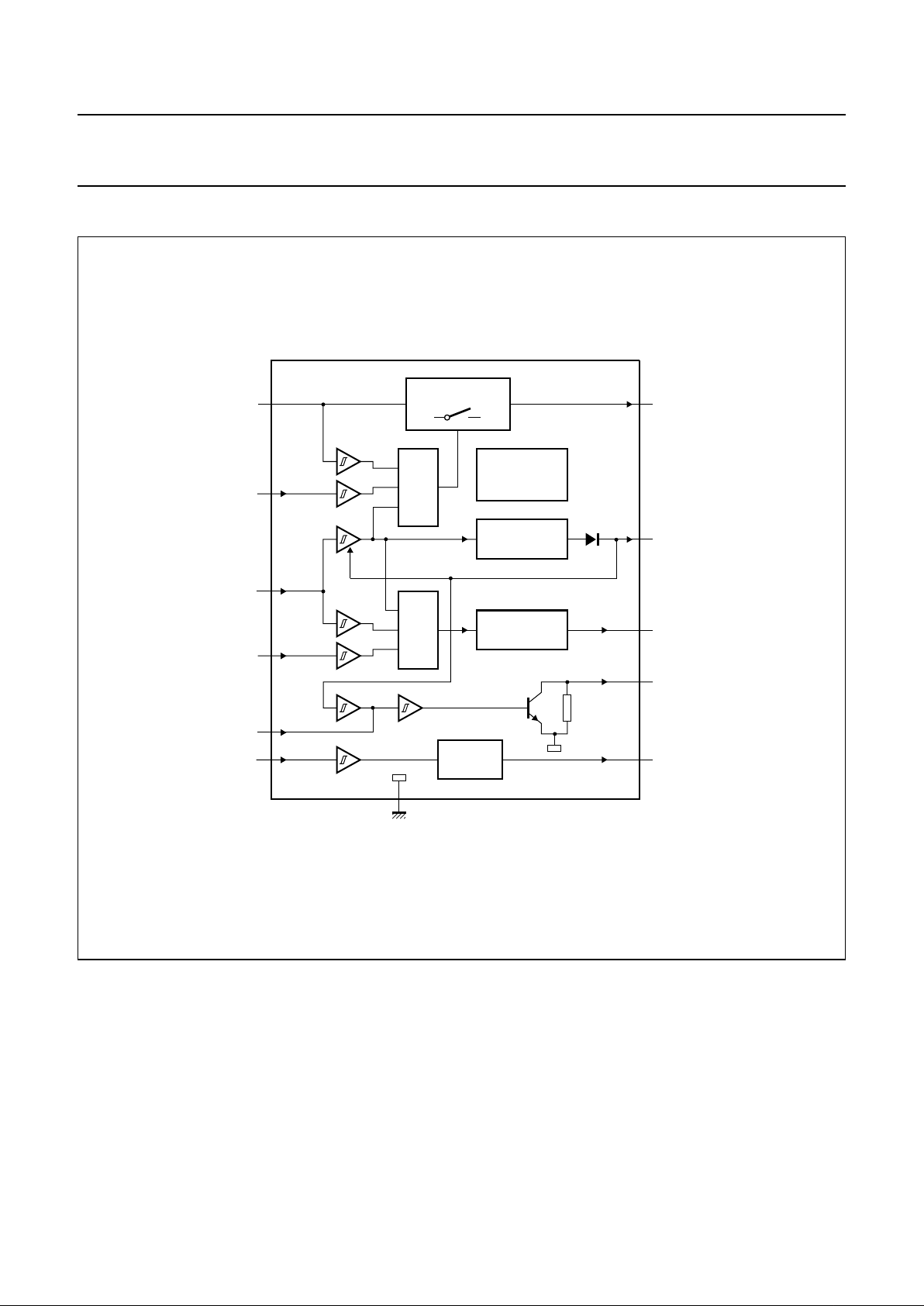
BLOCK DIAGRAM
Fig.1 Block diagram (for DBS13P package; SOT141-6).
handbook, full pagewidth
MBE237
REGULATOR 1
IGNITION
BUFFER
REGULATOR 2
11
13
4
5
8
TEMPERATURE
LOAD DUMP
PROTECTION
2
12
9
3
7
10
POWER SWITCH
&
&
ground
V
I(sw)
(14.4 V)
V
P
6
V
en(REG1)
V
en(sw)
TDA3604Q
V
I(ig)
C
RES
V
O(ig)
RES
(5 V)
REG1
(9 V/300 mA)
REG2
(5 V/50 mA)
V
O(sw)
(13.6 V/0.5 A)
1997 Aug 21 5
Philips Semiconductors Product specification
Multiple voltage regulators with external
reset delay and switch
TDA3604Q; TDA3604TH
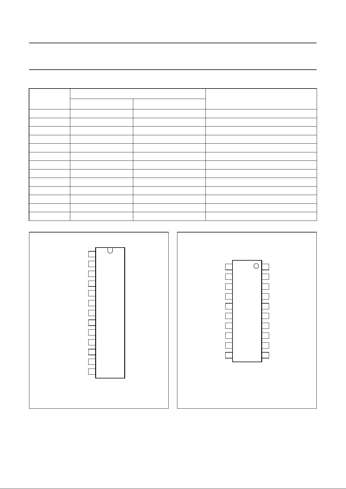
PINNING
SYMBOL
PIN
DESCRIPTION
SOT141-6 SOT418-2
n.c. 1 1, 2, 6, 9, 13, 18, 19 and 20 not connected
V
I(sw)
2 3 power switch input
V
P
3 4 supply voltage
REG1 4 5 regulator 1 output
RES 5 7 reset output (+5 V)
V
en(REG1)
6 8 regulator 1 enable input
V
en(sw)
7 10 power switch enable input
V
O(ig)
8 11 ignition output
C
RES
9 12 reset delay capacitor
GND 10 14 ground (0 V)
REG2 11 15 regulator 2 output
V
I(ig)
12 16 ignition input
V
O(sw)
13 17 power switch output
Fig.2 Pin configuration SOT141-6.
handbook, halfpage
TDA3604Q
MBE236
1
2
3
4
5
6
7
8
9
10
11
12
13
n.c.
l(sw)
V
REG1
REG2
RES
RES
GND
C
en(REG1)
V
en(sw)
V
O(ig)
V
I(ig)
V
O(sw)
V
P
V
Fig.3 Pin configuration SOT418-2.
handbook, halfpage
n.c.
n.c.
n.c.
V
O(sw)
V
I(ig)
REG2
GND
n.c.
C
RES
V
O(ig)
n.c.
n.c.
V
I(sw)
V
P
n.c.
RES
REG1
V
en(REG1)
n.c.
V
en(sw)
1
2
3
4
5
6
7
8
9
10
11
12
20
19
18
17
16
15
14
13
TDA3604TH
MGK596

1997 Aug 21 6
Philips Semiconductors Product specification
Multiple voltage regulators with external
reset delay and switch
TDA3604Q; TDA3604TH
FUNCTIONAL DESCRIPTION
The TDA3604Q and TDA3604TH are multiple output
voltage regulators with a power switch, intended for use in
car radios with or without a microcontroller. Because of
low-voltage operation of the car radio, low-voltage drop
regulators are used.
Regulator 2 will switch on when the supply voltage
exceeds 6.5 V for the first time and will switch off again
when the output voltage of regulator 2 drops below 1.9 V
(this is below an engine start). When regulator 2 is
switched on and the output voltage of this regulator is
within its voltage range, the reset output will be enabled
(reset will go HIGH via a pull-up resistor) to generate a
reset to the microcontroller. The reset cycles can be
extended by an external capacitor at C
RES
(pin of the reset
delay capacitor). The above mentioned start-up feature is
built-in to secure a smooth start-up of the microcontroller
at first connection, without uncontrolled switching of
regulator 2 during the start-up sequence.
When both regulator 2 and the supply voltage (V
P
> 4.5 V)
are available, regulator 1 and the power switch can be
operated by the enable inputs V
en(REG1)
and V
en(sw)
respectively.
All output pins are fully protected. The regulators are
protected against load dump (regulator 1 will switch off at
supply voltages higher than 25 V) and short-circuit
(foldback current protection).
The power switch contains a current protection which is
delayed for ≥10 ms (in short-circuit condition). During this
time the current is limited to 1.4 A (VP≤ 18 V).
At supply voltages over 16.9 V the power switch is
clamped at 15.0 V (to avoid externally connected circuitry
being damaged by an overvoltage) and the power switch
will switch off at load dump.
Interfacing with the microcontroller can be accomplished
by an ignition Schmitt trigger and ignition output buffer,
(simple full/semi on/off logic applications).
The total timing of a semi on/off logic set is shown in Fig.4.
 Loading...