

Philips tda3604 DATASHEETS

INTEGRATED CIRCUITS
DATA SH EET
TDA3604
Multiple voltage regulator with
external reset delay and switch
Preliminary specification
Supersedes data of 1995 Feb 16
File under Integrated Circuits, IC01
1995 Oct 04

Philips Semiconductors Preliminary specification
Multiple voltage regulator with external
reset delay and switch
FEATURES
• One VP state controlled regulator (regulator 2)
• Regulator 2, reset and ignition buffer operates during
load dump and thermal shutdown
• Separate control pins for switching regulator 1 and the
power switch
• Supply voltage range of −18 to 50 V (operating
from 9.75 V)
• Low reverse current of regulator 2
• Low quiescent current (when regulator 1 is switched off,
standby)
• Ignition input/output
• Reset output
• Reset delay time adjustable
• High ripple rejection
• Power switch
• Separate supply for the power switch.
PROTECTIONS
TDA3604
GENERAL DESCRIPTION
The TDA3604 is a multiple output voltage regulator with a
power switch, intended for use in car radios with or without
a microcontroller.
It contains one fixed voltage regulator with a foldback
current protection (regulator 1) and one fixed voltage
regulator (regulator 2), intended to supply a
microcontroller, that also operates during load dump and
thermal shutdown.
There is a power switch with protections, operated by an
enable input.
The reset and ignition outputs can be used to interface by
the microcontroller. The reset-signal can be used to call up
the microcontroller and the ignition output indicates
ignition voltage available.
Both supply pins can withstand load dump pulses and
negative supply voltages.
Regulator 2 will be switched on at a supply voltage >6.5 V
and off at a voltage of regulator 2 <1.9 V.
• Reverse polarity safe (down to −18 V without high
reverse current)
• Able to withstand voltages up to 18 V at the outputs
(supply line may be shortened)
• ESD protected on all pins
• Thermal protection
• Load dump protection
• Foldback current limit protection for regulators 1 and 2
• Delayed second current limit protection for the power-
switch
• The regulator outputs and the power switch are DC
short-circuited safe to ground and V
ORDERING INFORMATION
TYPE NUMBER
NAME DESCRIPTION VERSION
TDA3604 DBS13P plastic DIL-bent-SIL power package; 13 leads (lead length 12 mm) SOT141-6
.
P
PACKAGE
1995 Oct 04 2
Philips Semiconductors Preliminary specification
Multiple voltage regulator with external
TDA3604
reset delay and switch
QUICK REFERENCE DATA
SYMBOL PARAMETER CONDITIONS MIN. TYP. MAX. UNIT
Supply
V
P
I
q
T
vj
Voltage regulators
V
REG1
V
REG2
V
drop(REG1)
Power switch
V
drop(sw)
I
M
supply voltage
operating 9.75 14.4 25 V
regulator 2 on note 1 2.4 14.4 25 V
jump start t ≤ 10 minutes −−30 V
load dump protection during 50 ms; t
≥ 2.5 ms −−50 V
r
total quiescent current standby mode − 400 500 µA
operating virtual junction temperature −−150 °C
output voltage regulator 1 0.5 mA ≤ I
output voltage regulator 2 0.5 mA ≤ I
≤ 300 mA 8.65 9.0 9.35 V
REG1
REG2
≤ 30 mA;
4.8 5.0 5.2 V
VP= 14.4 V
drop-out voltage I
= 0.3 A; note 2 −−0.5 V
REG1
drop-out voltage Isw= 0.5 A; note 3 −−1.4 V
peak current t ≤ 10 ms 1.4 −−A
Notes
1. Minimum operating voltage, only if V
2. The drop-out voltage of regulator 1 is measured between VPand V
has exceeded 6.5 V.
P
REG 1.
3. The drop-out voltage of the power switch is measured between VPand Vsw.
1995 Oct 04 3
Philips Semiconductors Preliminary specification
Multiple voltage regulator with external
reset delay and switch
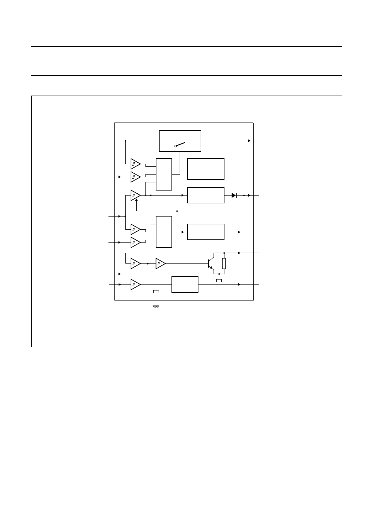
BLOCK DIAGRAM
ndbook, full pagewidth
V
l(sw)
(14.4 V)
V
en(sw)
V
en(REG1)
2
7
3
V
P
6
POWER SWITCH
&
&
TEMPERATURE
LOAD DUMP
PROTECTION
REGULATOR 2
REGULATOR 1
TDA3604
13
11
4
5
V
O(sw)
(13.6 V/0.5 A)
REG2
(5 V/30 mA)
REG1
(9 V/300 mA)
RES
(5 V)
TDA3604
l(ig)
9
12
IGNITION
BUFFER
10
ground
MBE237
8
V
O(ig)
C
RES
V
Fig.1 Block diagram.
1995 Oct 04 4
Philips Semiconductors Preliminary specification
Multiple voltage regulator with external
reset delay and switch
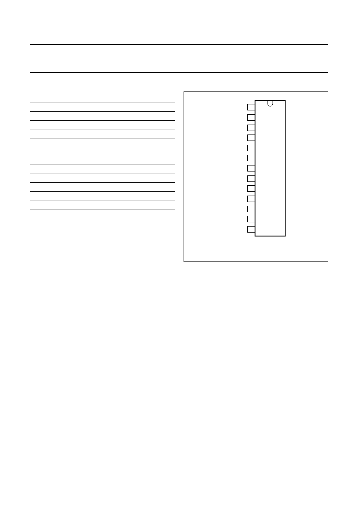
PINNING
SYMBOL PIN DESCRIPTION
n.c. 1 not connected
V
I(sw)
V
P
REG1 4 regulator 1 output
RES 5 reset output voltage (+5 V)
V
en(REG1)
V
en(sw)
V
O(ig)
C
RES
GND 10 ground (0 V)
REG2 11 regulator 2 output
V
I(ig)
V
O(sw)
2 power switch input voltage
3 supply voltage
6 regulator 1 enable input
7 power switch enable input voltage
8 ignition output voltage
9 reset capacitor
12 ignition input voltage
13 power switch output voltage
handbook, halfpage
V
en(REG1)
V
REG1
V
en(sw)
V
C
REG2
V
O(sw)
n.c.
l(sw)
RES
O(ig)
RES
GND
V
I(ig)
TDA3604
1
2
V
3
P
4
5
6
7
TDA3604
8
9
10
11
12
13
MBE236
Fig.2 Pin configuration.
1995 Oct 04 5
 Loading...