

Philips TDA3602-N3 Datasheet
DATA SH EET
Product specification
File under Integrated Circuits, IC01
July 1994
INTEGRATED CIRCUITS
TDA3602
Multiple output voltage regulator

July 1994 2
Philips Semiconductors Product specification
Multiple output voltage regulator TDA3602
FEATURES
• Two VP state controlled regulators (REG1 and REG2)
• Regulator 3 operates during load dump or thermal
shutdown
• Multi-function control pin
• A back-up circuit for Regulator 3 via a single capacitor
• Supply voltage of −6 V to 50 V (a voltage of −3 V on V
P
does not discharge capacitor Cbu)
• Low reverse current Regulator 3
• Low quiescent current in coma mode
• HOLD output
• RESET output (LOW at load dump)
• High ripple rejection.
PROTECTIONS
• Foldback current limit protection (Regulators 1 and 2)
• Load dump protection
• Thermal protection
• DC short-circuit safe to ground and V
P
of all regulator
outputs
• Reverse polarity safe of pin 1 (VP). No high currents are
flowing which can damage the IC
• Capable of handling high energy on the regulator
outputs.
GENERAL DESCRIPTION
The TDA3602 is a multiple output voltage regulator,
intended for use in car radios with or without a
microprocessor. It contains two fixed voltage regulators
with foldback current protection (Regulators 1 and 2), and
one fixed voltage regulator that also operates during load
dump and thermal shutdown. This regulator can be used
to supply a microprocessor.
A back-up circuit supplies Regulator 3 during a short
period after the power is cut off (negative field decay or
engine start procedure). A state control pin (pin 4) controls
the device, which can be switched through four stages
using the information at this pin. The switching levels at
this pin contain hysteresis.
RESET and HOLD outputs can be used to interface with a
microprocessor. The RESET signal can be used to call up
or initialize a microprocessor (power-on reset). The HOLD
signal can be used to control the power stages (mute
signal in a low end application), or to generate a HOLD
interrupt (microprocessor application).
An internal Zener diode on the back-up pin allows this pin
to withstand a load dump when supplied by the pin using a
100 Ω series resistor.
The supply pin can withstand load dump pulses and
negative supply voltages.
July 1994 3
Philips Semiconductors Product specification
Multiple output voltage regulator TDA3602
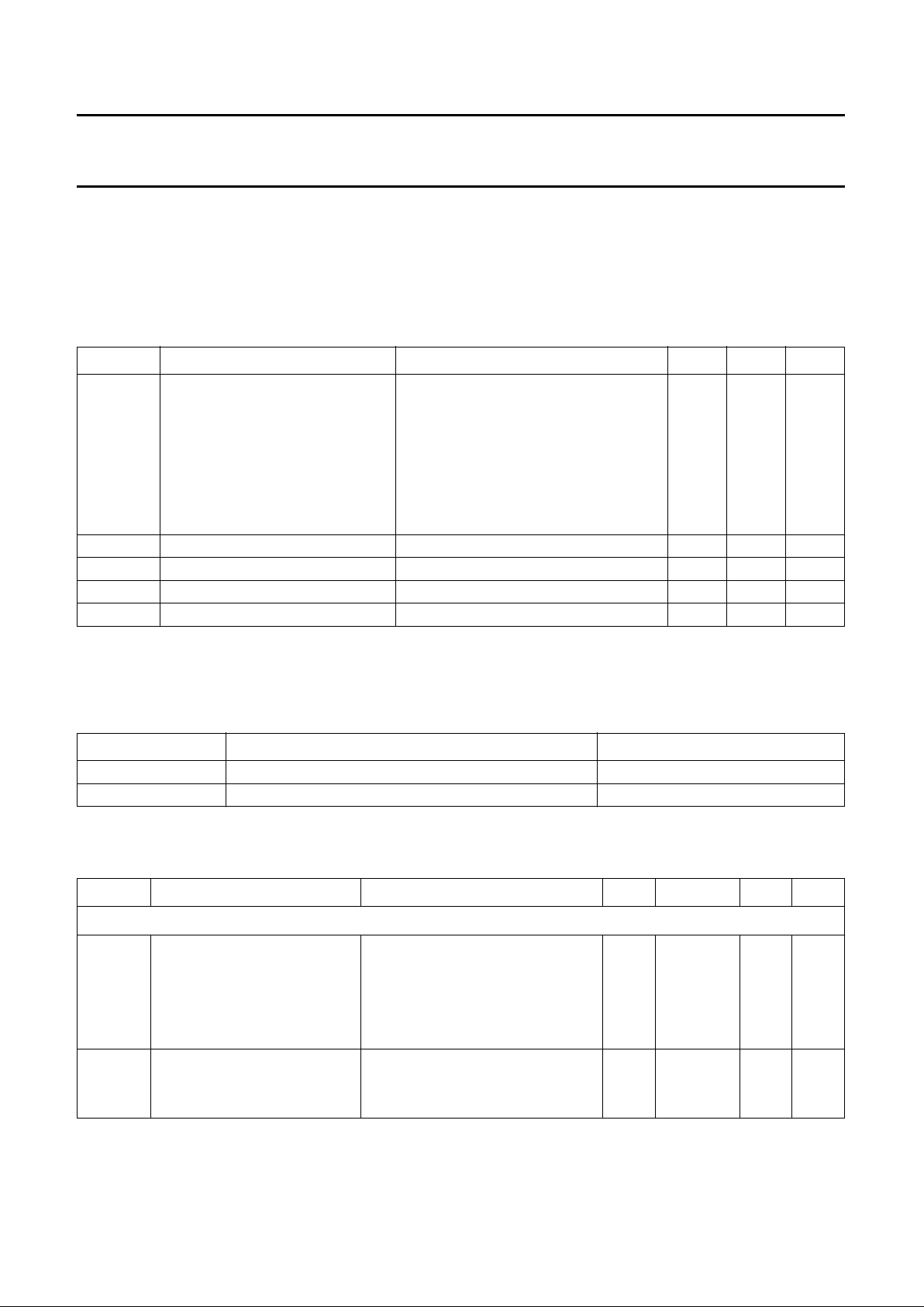
QUICK REFERENCE DATA
Note
1. Vbu (pin 8) supplied by VP2 with a 100 Ω series resistor and I
REG3
< 10 mA.
ORDERING INFORMATION
Note
1. SOT110-1; 1996 August 21.
SYMBOL PARAMETER CONDITIONS MIN. TYP. MAX. UNIT
Supply
V
P
positive supply voltage
operating 9.2 14.4 18 V
Regulator 3 on 6.0 14.4 18 V
jump start −−30 V
load dump; Regulator 3 on −−50 V
operating note 1 6.5 − 30 V
load dump; Regulator 3 on note 1 −−50 V
I
P
total quiescent current coma mode − 290 −µA
T
vj
virtual junction temperature −−150 °C
Voltage regulators
V
R1
output voltage Regulator 1 0.5 mA ≤ IR1≤ 250 mA 8.2 8.5 8.8 V
V
R2
output voltage Regulator 2 0.5 mA ≤ IR2≤ 140 mA 4.8 5.0 5.2 V
V
R3
output voltage Regulator 3 0.5 mA ≤ IR3≤ 50 mA 4.8 5 5.2 V
EXTENDED TYPE
NUMBER
PACKAGE
PINS PIN POSITION MATERIAL CODE
TDA3602
(1)
9 SIL plastic SOT110
July 1994 4
Philips Semiconductors Product specification
Multiple output voltage regulator TDA3602
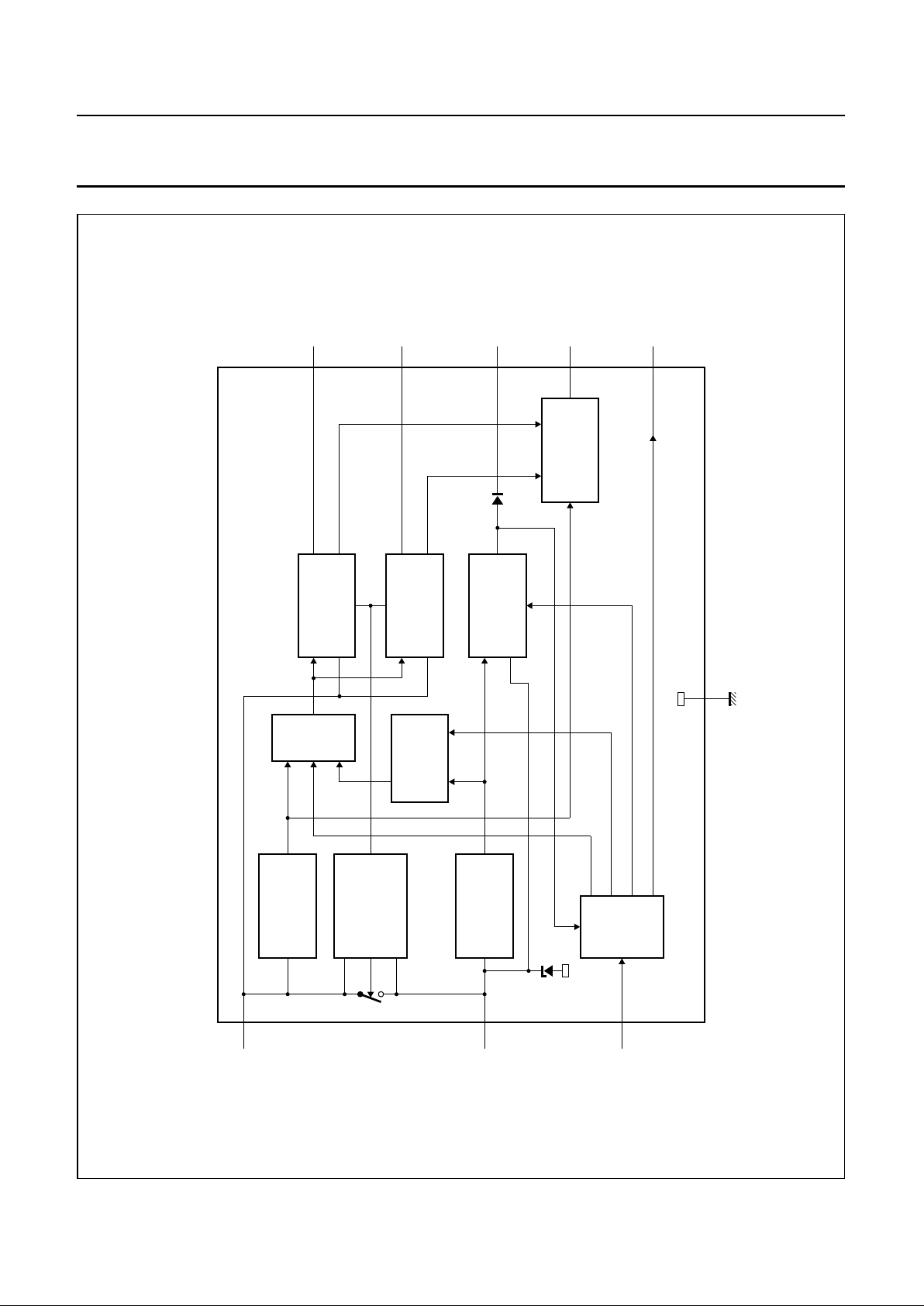
handbook, full pagewidth
REGULATOR 2
SCHMITT
TRIGGER
V
P
MCD346 - 1
&
SCHMITT
TRIGGER
V
bu
PROTECTION
LOADDUMP /
V REVERSE
bu
POLARITY
STATE
CONTROL
CIRCUIT
6
ground
REGULATOR 1
2
REGULATOR 3
5
HOLD CIRCUIT
CONTROL
9
7
Q
RS
1
8
4
R1,R2 on
> 2 V
L / H current
reset
V 8.5 V
hold
reset
3
TDA3602
5 V switched
(back up)
V
bu
(state control)
V
sc
V
sc
V
P
&
V
bu
Zener
(21 V)
REG1
V 5 V
REG2
V 5 V
REG3
Fig.1 Block diagram.
July 1994 5
Philips Semiconductors Product specification
Multiple output voltage regulator TDA3602
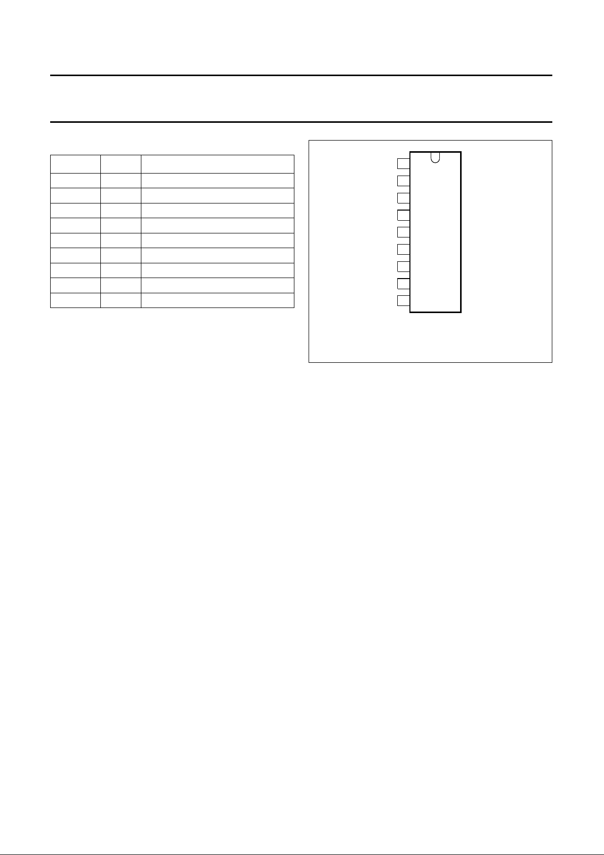
PINNING
SYMBOL PIN DESCRIPTION
V
P
1 positive supply voltage
REG1 2 Regulator 1 output
RESET 3 reset output
V
sc
4 state control input
HOLD 5 hold output
GND 6 ground
REG3 7 Regulator 3 output
V
bu
8 back-up
REG2 9 Regulator 2 output
handbook, halfpage
MCD345
1
2
3
4
5
6
7
8
9
P
V
GND
REG1
REG3
REG2
TDA3602
sc
V
bu
V
RESET
HOLD
Fig.2 Pin configuration.
FUNCTIONAL DESCRIPTION
This multiple output voltage regulator contains three fixed
voltage regulators, numbered 1, 2 and 3. Two of these can
be switched between the on and off states using the state
control pin (pin 4). The third (Regulator 3), which is
continuously in, can be switched by the state control pin
between a low and a high current mode.
In addition to Regulators 1 and 2, the device is supplied by
an internal switch that is open when the supply voltage
falls below the back-up voltage (negative field decay or
engine start procedure), or during a load dump. (During
this load dump, Regulators 1 and 2 are switched off and
RESET is switched LOW). This switched supply voltage
(the so-called back-up voltage (Vbu), is available at pin 8.
An electrolytic capacitor can be connected to this pin, and
the charge on this capacitor can be used to supply the
device for a short period after the supply voltage is
removed.
Three pins are provided for interfacing with a
microprocessor:
• state control pin
• hold output pin
• reset output pin.
When the supply voltage (VP) is connected to the device,
Vbu will rise. When Vbu reaches 7.9 V, the device is in the
power-on mode. The RESET output goes HIGH and
Regulator 3 is switched on. In a microprocessor
application, the RESET output can be used to call up the
CPU and to initialize the program.
What follows depends on the voltage at the state control
pin (V
sc
). In most applications, when the supply voltage is
connected, Vsc will rise slowly (e.g. by charging a
capacitor).The device will leave the power-on mode and
enter the reset mode when Vsc rises above 2.2 V. In both
the power-on and reset modes, Regulator 3 will be in the
high current mode, Regulators 1 and 2 will be switched off
and the RESET output will be HIGH.
The device will enter the wake mode when Vsc reaches 2.8
V. The RESET pin will go LOW and the CPU must be
switched to the sleep mode. Regulator 3 is still in the high
current mode.
As Vsc continues rising and the voltage reaches 3.6 V, the
stabilizer will be switched into the sleep mode. It will be in
a coma mode when Vsc is greater than 3.8 V. In this mode,
only the relevant circuits remain operating; this is to keep
the power consumption as low as possible i.e. typically 290
µA.
If the device is switched on with Vsc already higher than 3.8
V, the device will be switched directly from the power-on
mode into the coma mode.
When Vsc is lowered gradually from 3.6 V (or higher) to 2
V, the device will go from sleep to reset again.
Vsc must be lower than 1.1 V to bring the device into the on
mode; note that this is not the same as the power-on
mode. In this condition, Regulator 3 is in the high current
mode, both Regulators 1 and 2 are switched on and the
HOLD output will be HIGH (depending on the state of V
P
and the in-regulation condition of Regulators 1 and 2).
July 1994 6
Philips Semiconductors Product specification
Multiple output voltage regulator TDA3602
When the device is in the on mode, it will switch back to the reset mode when Vsc rises to 2 V, or when the supply voltage
drops below 7.3 V.
When V
REG3
drops below 3 V, the device will return to the power off mode, regardless of the condition the device was in.
LIMITING VALUES
In accordance with the Absolute Maximum Rating System (IEC 134).
Note
1. V
bu
(pin 8) supplied by VP2 with a 100 Ω series resistor and I
REG3
< 10 mA.
THERMAL RESISTANCE
CHARACTERISTICS
V
P
= 14.4 V; T
amb
= 25 °C; measured in Fig.6; unless otherwise specified.
SYMBOL PARAMETER CONDITIONS MIN. MAX. UNIT
V
P
supply voltage
operating − 18 V
jump start t ≤ 10 min − 30 V
load dump t ≤ 50 ms; t
r
≥ 2.5 ms − 50 V
Regulator 3 on V
P
> −3 V; note 1 − 30 V
load dump t ≤50 ms; t
r
≥ 2.5 ms; note 1 − 50 V
reverse battery voltage −6 − V
T
stg
storage temperature non-operating −55 +150 °C
T
vj
virtual junction temperature operating −40 +150 °C
V
pr
reverse polarity non-operating − 6V
P
tot
total power dissipation − 15 W
SYMBOL PARAMETER THERMAL RESISTANCE
R
th j-a
from junction to ambient in free air 50 K/W
R
th j-c
from junction to case (see Fig.6) 12 K/W
SYMBOL PARAMETER CONDITIONS MIN. TYP. MAX. UNIT
Supply
V
P
supply voltage
operating 9.2 14.4 18 V
Regulator 3 on note 1 6.0 14.4 18 V
jump start t ≤ 10 min −− 30 V
load dump t ≤ 50 ms; t
r
≥ 2.5 ms −− 50 V
I
P
quiescent current Vsc > 4V; note 2
V
P
= 12.4 V − 280 360 µA
V
P
= 14.4 V − 290 −µA
July 1994 7
Philips Semiconductors Product specification
Multiple output voltage regulator TDA3602
Schmitt triggers
VP2SCHMITT TRIGGER (FOR HOLD AND REGULATORS 1 AND 2)
V
thr
rising voltage threshold 7.3 7.6 8.0 V
V
thf
falling voltage threshold 6.8 7.1 7.5 V
V
hy
hysteresis − 0.5 − V
REGULATOR 1SCHMITT TRIGGER (FOR HOLD)
V
thr
rising voltage threshold − VR1 − 0.2 − V
V
thf
falling voltage threshold − VR1 − 0.3 − V
V
hy
hysteresis − 0.1 − V
REGULATOR 2SCHMITT TRIGGER (FOR HOLD)
V
thr
rising voltage threshold − VR2 − 0.2 − V
V
thf
falling voltage threshold − VR2 − 0.3 − V
V
hy
hysteresis − 0.1 − V
VBU SCHMITT TRIGGER (REGULATOR 3)
V
thr
rising voltage threshold V
bu
7.3 7.9 8.4 V
V
thf
falling voltage threshold V
REG3
2.5 3 3.5 V
V
hy
hysteresis − 4.9 − V
State control pin
V
th
voltage threshold between note 2 − V
thr1
+ 0.2 − V
sleep and coma
V
thr1
voltage threshold wake to 3.35 3.6 3.85 V
sleep
V
thf1
voltage threshold sleep to 2.5 2.7 2.9 V
wake
V
hy1
hysteresis wake/sleep 0.85 0.92 1.0 V
V
thr2
voltage threshold reset to 2.6 2.8 3.0 V
wake
V
thf2
] voltage threshold wake to 1.75 1.9 2.05 V
reset
V
hy2
hysteresis reset/wake 0.85 0.92 1.0 V
V
thr3
voltage threshold on to reset 1.85 2.0 2.15 V
V
thf3
voltage threshold reset to on 1.0 1.1 1.2 V
V
hy3
hysteresis on/reset 0.85 0.92 1.0 V
I
scl
input current
V
sc
≤ 0.8 V −− −1µA
V
sc
≥ 4 V −− 1µA
SYMBOL PARAMETER CONDITIONS MIN. TYP. MAX. UNIT
July 1994 8
Philips Semiconductors Product specification
Multiple output voltage regulator TDA3602
Reset output
V
OL
LOW level output voltage IOL = 0 0 0.2 0.8 V
V
OH
HIGH level output voltage 2.0 5.0 5.25 V
I
OL
LOW level output current VOL ≤ 0.8 V 0.3 0.8 − mA
I
OH
HIGH level output current VOH > 3 V −0.3 −2.0 − mA
Hold output
V
OL
LOW level output voltage IOL = 0 0 0.2 0.8 V
V
OH
HIGH level output voltage 2.0 5.0 5.25 V
I
OL
LOW level output current VOL ≤ 0.8 V; note 3 0.3 1.0 − mA
I
OH
HIGH level output current VOH > 3 V −1.5 −9.0 − mA
Regulator 1 (I
REG1
= 5 mA unless otherwise specified)
V
REG1
output voltage off Vsc > 2.1 V − 1 400 mV
V
REG1
output voltage
0.5 V ≤ I
REG1
≤ 250 mA 8.2 8.5 8.8 V
10 V ≤ V
P
≤ 18 V 8.2 8.5 8.8 V
∆V
REG1
line regulation 10 V ≤ VP ≤ 18 V −− 50 mV
∆V
REGL1
load regulation 0.5 mA ≤ I
REG1
≤ 250 mA −− 50 mV
SVRR1 supply voltage ripple rejection f = 200 Hz;2 V (p-p) 60 −−dB
V
REGd1
drop-out voltage I
REG1
= 250 mA −− 0.4 V
I
REGm1
current limit V
REG1
> 7 V; note 4 0.4 − 1.2 A
I
REGsc1
short-circuit current RL ≤ 0.5 Ω; note 4 − 250 − mA
Regulator 2 (I
REG2
= 10 mA unless otherwise specified)
V
REG2
output voltage off Vsc >2.1 V − 1 400 mV
V
REG2
output voltage
0.5 V ≤ I
REG2
≤ 140 mA 4.8 5.0 5.2 V
8 V ≤ V
P
≤ 18 V 4.8 5.0 5.2 V
∆V
REG2
line regulation 8 V ≤ VP ≤ 18 V −− 50 mV
∆V
REGL2
load regulation 0.5 mA ≤ I
REG2
≤ 140 mA −− 50 mV
SVRR2 supply voltage ripple rejection f = 200 Hz; 2 V (p-p) 60 −−dB
V
REGd2
drop-out voltage I
REG2
= 140 mA − 1.2 − V
I
REGm2
current limit V
REG2
> 4.5 V; note 4 200 − 600 mA
I
REGsc2
short-circuit current RL ≤ 0.5 Ω; note 4 − 130 − mA
SYMBOL PARAMETER CONDITIONS MIN. TYP. MAX. UNIT
 Loading...