

Philips TDA3601Q-N2-S3, TDA3601Q-N2, TDA3601AQ-N2-S3, TDA3601AQ-N2 Datasheet

DATA SH EET
Product specification
Supersedes data of September 1994
File under Integrated Circuits, IC01
1995 Dec 13
INTEGRATED CIRCUITS
TDA3601Q
TDA3601AQ
Multiple output voltage regulators
1995 Dec 13 2
Philips Semiconductors Product specification
Multiple output voltage regulators
TDA3601Q
TDA3601AQ
FEATURES
• Six fixed voltage regulators
• Three microprocessor-controlled regulators
• Two VP-state controlled regulators
• One fixed voltage regulator (can operate during load
dump or thermal shutdown)
• VP1 supply pin (low current pin)
• VP2 supply pin (high current pin)
• RESET output (TDA3601Q) or RESET output
(TDA3601AQ)
• Internally fixed timer of 100 µs
• Externally fixed delay timer
• High ripple rejection
• Flexible leads.
PROTECTION
• Current limit protection for regulator 1
• Foldback current limit protection (regulators 2 to 6)
• Load dump protection
• Thermal protection
• Regulator outputs DC short-circuit-safe to ground,
VP and other regulator outputs
• Capable of handling high energy on any of the
output pins
• Reverse polarity safe.
QUICK REFERENCE DATA
Notes
1. Load dump, during 50 ms, t
r
> 2.5 ms.
2. Regulator 1 operating, 0.5 mA ≤ IR1≤ 20 mA.
3. VP1 = 13.2 V; VP2 = R4-sel = R5-sel = 0; IR1=0.
SYMBOL PARAMETER CONDITIONS MIN. TYP. MAX. UNIT
Entire device
V
P1
supply voltage range operating 11 13.2 18 V
load dump; notes 1 and 2 −−50 V
V
P2
supply voltage range operating 11 13.2 18 V
non-operating −−30 V
load dump; note 1 −−50 V
I1
tot
total quiescent current, V
P1
VP2= 0; note 3 − 1 1.4 mA
T
c
crystal temperature −−150 °C
Voltage regulators
V
R1
output voltage regulator 1 0.5 mA ≤ IR1≤ 20 mA 4.75 5 5.25 V
V
R2
output voltage regulator 2 5 mA ≤ IR2≤ 200 mA 1.9 2.1 2.3 V
V
R3
output voltage regulator 3 5 mA ≤ IR3≤ 150 mA 4.75 5 5.25 V
V
R4
output voltage regulator 4 5 mA ≤ IR4≤ 150 mA 9 9.5 10 V
V
R5
output voltage regulator 5 5 mA ≤ IR5≤ 200 mA 9 9.5 10 V
V
R6
output voltage regulator 6 5 mA ≤ IR6≤ 200 mA 9.3 9.75 10.2 V
1995 Dec 13 3
Philips Semiconductors Product specification
Multiple output voltage regulators
TDA3601Q
TDA3601AQ
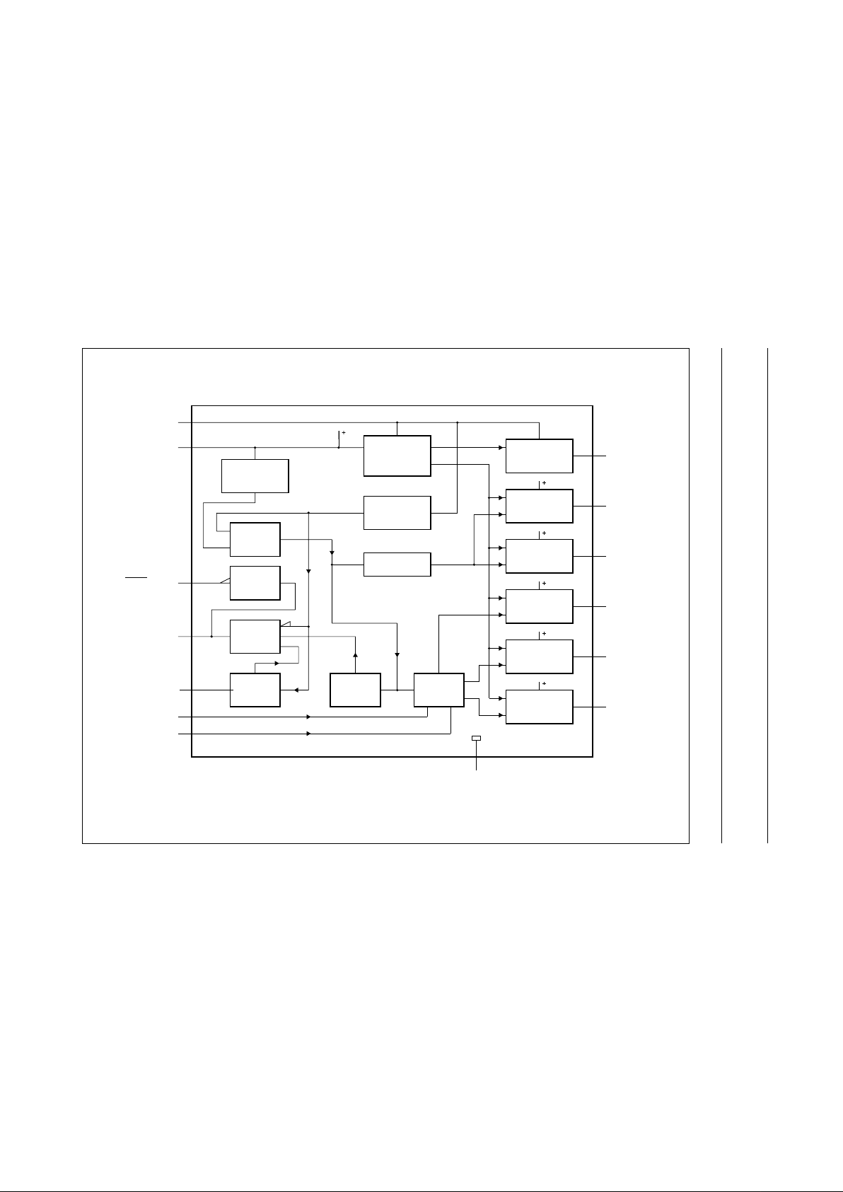
BLOCK DIAGRAM
handbook, full pagewidth
REGULATOR 1
5 V
REGULATOR 2
2.1 V
REGULATOR 3
5 V
REGULATOR 4
9.5 V
REGULATOR 5
9.5 V
REGULATOR 6
9.75 V
OVER VOLTAGE
AND THERMAL
SHUTDOWN
OUT OF
REGULATION
POWER ON
INVERT
ONE SHOT
40 ms
LOGIC
SWITCH
ONE SHOT
100 µs
OR GATE
AND
SENSE
V
P2
4
regulator 1
output
10
regulator 2
output
9
regulator 3
output
6
regulator 4
output
7
regulator 5
output
8
regulator 6
output
12
ground
V
P1
V
P2
5
11
13A
13
1
2
3
RESET - output
regulator 4
select
regulator 5
select
RESET - output
TDA3601Q
TDA3601AQ
MCD341
reset timing
capacitor
Fig.1 Block diagram.
1995 Dec 13 4
Philips Semiconductors Product specification
Multiple output voltage regulators
TDA3601Q
TDA3601AQ
ORDERING INFORMATION
TYPE NUMBER
PACKAGE
NAME DESCRIPTION VERSION
TDA3601Q
DBS13P plastic DIL-bent-SIL power package; 13 leads (lead length 12 mm) SOT141-6
TDA3601AQ
GENERAL DESCRIPTION
The circuit contains five fixed voltage regulators with
foldback current protection and one fixed voltage regulator
(REGULATOR 1) that also operates during a load dump.
In addition, a RESET function (TDA3601Q) or RESET
function (TDA3601AQ), timer functions and a logic
multiplexer are implemented.
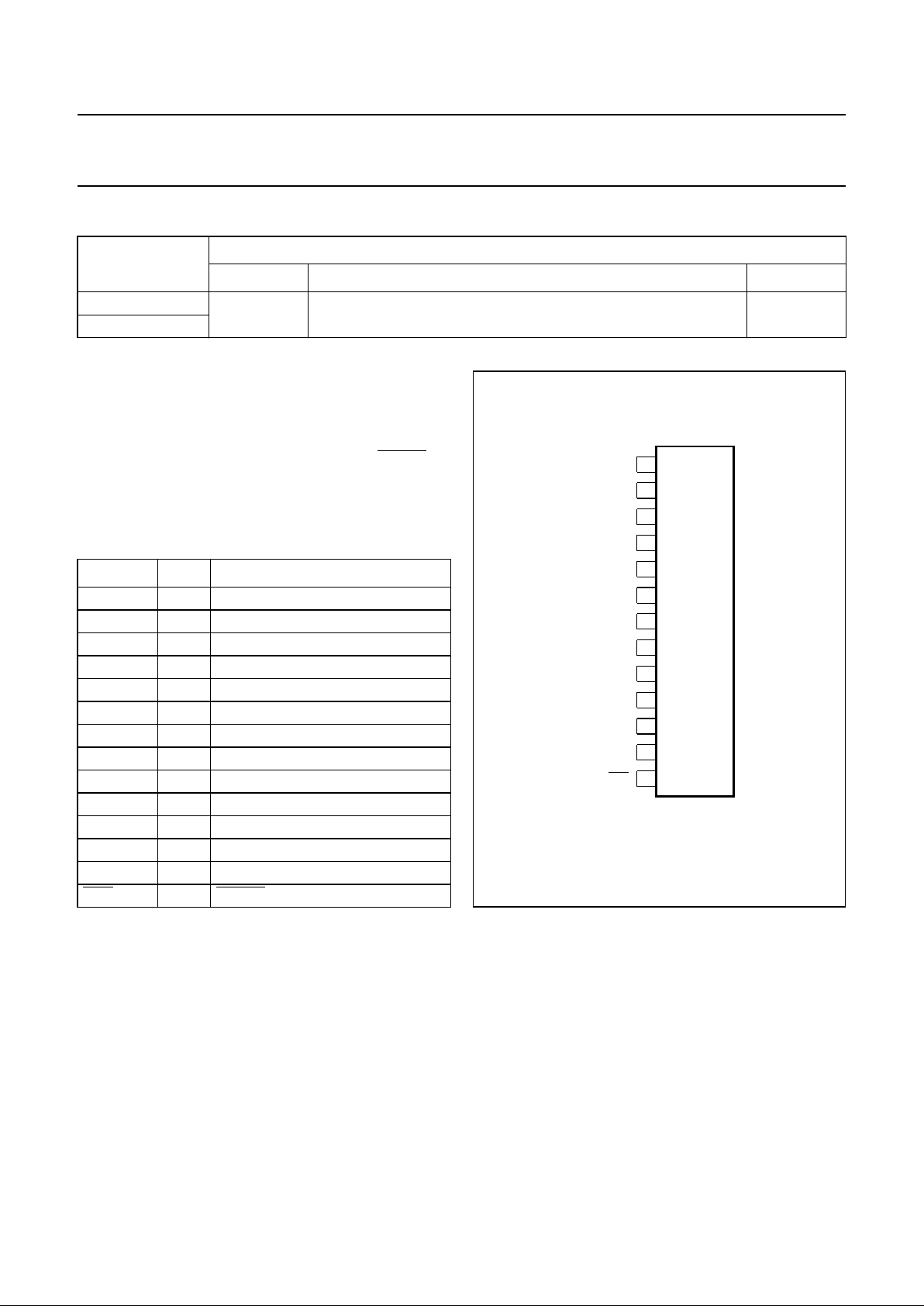
PINNING
SYMBOL PIN DESCRIPTION
C
RESET
1 reset timing capacitor
R5-sel 2 regulator 5 select
R4-sel 3 regulator 4 select
REG1 4 regulator 1 output (5 V)
V
P1
5 supply voltage
REG4 6 regulator 4 output (9.5 V)
REG5 7 regulator 5 output (9.5 V)
REG6 8 regulator 6 output (9.75 V)
REG3 9 regulator 3 output (5 V)
REG2 10 regulator 2 output (2.4 V)
V
P2
11 supply voltage
GND 12 ground
RES 13 RESET output (TDA3601Q)
RES 13A RESET output (TDA3601AQ)
Fig.2 Pin configuration.
andbook, halfpage
MCD340 - 1
1
2
3
4
5
6
7
8
9
10
11
12
13
P1
V
GND
P2
V
TDA3601Q
TDA3601AQ
C
RESET
R5 - sel
REG1
REG4
R4 - sel
REG5
REG6
REG3
REG2
RES or RES
 Loading...