

Philips TDA3601Q, TDA3601AQ Datasheet

INTEGRATED CIRCUITS
DATA SH EET
TDA3601Q
TDA3601AQ
Multiple output voltage regulators
Product specification
Supersedes data of September 1994
File under Integrated Circuits, IC01
1995 Dec 13
Philips Semiconductors Product specification
Multiple output voltage regulators
FEATURES
• Six fixed voltage regulators
• Three microprocessor-controlled regulators
• Two VP-state controlled regulators
• One fixed voltage regulator (can operate during load
dump or thermal shutdown)
• VP1 supply pin (low current pin)
• VP2 supply pin (high current pin)
• RESET output (TDA3601Q) or RESET output
(TDA3601AQ)
• Internally fixed timer of 100 µs
• Externally fixed delay timer
• High ripple rejection
• Flexible leads.
QUICK REFERENCE DATA
TDA3601Q
TDA3601AQ
PROTECTION
• Current limit protection for regulator 1
• Foldback current limit protection (regulators 2 to 6)
• Load dump protection
• Thermal protection
• Regulator outputs DC short-circuit-safe to ground,
VP and other regulator outputs
• Capable of handling high energy on any of the
output pins
• Reverse polarity safe.
SYMBOL PARAMETER CONDITIONS MIN. TYP. MAX. UNIT
Entire device
V
P1
supply voltage range operating 11 13.2 18 V
load dump; notes 1 and 2 −−50 V
V
P2
supply voltage range operating 11 13.2 18 V
non-operating −−30 V
load dump; note 1 −−50 V
I1
tot
T
c
total quiescent current, V
P1
VP2= 0; note 3 − 1 1.4 mA
crystal temperature −−150 °C
Voltage regulators
V
R1
V
R2
V
R3
V
R4
V
R5
V
R6
output voltage regulator 1 0.5 mA ≤ IR1≤ 20 mA 4.75 5 5.25 V
output voltage regulator 2 5 mA ≤ IR2≤ 200 mA 1.9 2.1 2.3 V
output voltage regulator 3 5 mA ≤ IR3≤ 150 mA 4.75 5 5.25 V
output voltage regulator 4 5 mA ≤ IR4≤ 150 mA 9 9.5 10 V
output voltage regulator 5 5 mA ≤ IR5≤ 200 mA 9 9.5 10 V
output voltage regulator 6 5 mA ≤ IR6≤ 200 mA 9.3 9.75 10.2 V
Notes
1. Load dump, during 50 ms, t
> 2.5 ms.
r
2. Regulator 1 operating, 0.5 mA ≤ IR1≤ 20 mA.
3. VP1 = 13.2 V; VP2 = R4-sel = R5-sel = 0; IR1=0.
1995 Dec 13 2
1995 Dec 13 3
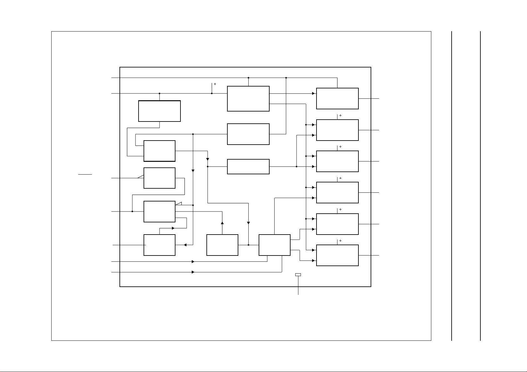
BLOCK DIAGRAM
Philips Semiconductors Product specification
Multiple output voltage regulators
V
P1
V
P2
RESET - output
RESET - output
reset timing
capacitor
regulator 5
select
regulator 4
select
5
11
13A
13
1
2
3
V
P2
SENSE
AND
INVERT
OR GATE
ONE SHOT
40 ms
TDA3601Q
TDA3601AQ
ONE SHOT
100 µs
OVER VOLTAGE
AND THERMAL
SHUTDOWN
OUT OF
REGULATION
POWER ON
LOGIC
SWITCH
12
ground
REGULATOR 1
5 V
REGULATOR 2
2.1 V
REGULATOR 3
5 V
REGULATOR 4
9.5 V
REGULATOR 5
9.5 V
REGULATOR 6
9.75 V
10
MCD341
4
regulator 1
output
regulator 2
output
9
regulator 3
output
6
regulator 4
output
7
regulator 5
output
8
regulator 6
output
TDA3601AQ
TDA3601Q
Fig.1 Block diagram.
handbook, full pagewidth
Philips Semiconductors Product specification
Multiple output voltage regulators
ORDERING INFORMATION
TYPE NUMBER
TDA3601Q
TDA3601AQ
GENERAL DESCRIPTION
The circuit contains five fixed voltage regulators with
foldback current protection and one fixed voltage regulator
(REGULATOR 1) that also operates during a load dump.
In addition, a RESET function (TDA3601Q) or RESET
function (TDA3601AQ), timer functions and a logic
multiplexer are implemented.
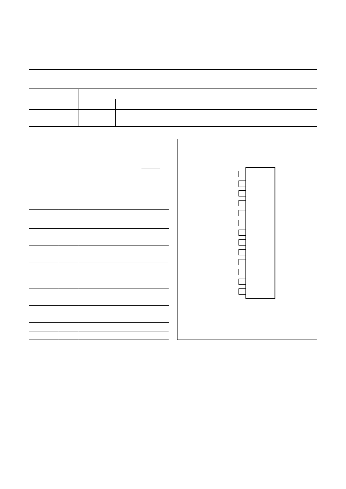
PINNING
SYMBOL PIN DESCRIPTION
C
RESET
1 reset timing capacitor
R5-sel 2 regulator 5 select
R4-sel 3 regulator 4 select
REG1 4 regulator 1 output (5 V)
V
P1
5 supply voltage
REG4 6 regulator 4 output (9.5 V)
REG5 7 regulator 5 output (9.5 V)
REG6 8 regulator 6 output (9.75 V)
REG3 9 regulator 3 output (5 V)
REG2 10 regulator 2 output (2.4 V)
V
P2
11 supply voltage
GND 12 ground
RES 13 RESET output (TDA3601Q)
RES 13A RESET output (TDA3601AQ)
NAME DESCRIPTION VERSION
DBS13P plastic DIL-bent-SIL power package; 13 leads (lead length 12 mm) SOT141-6
PACKAGE
andbook, halfpage
C
RESET
R5 - sel
R4 - sel
RES or RES
REG1
V
P1
REG4
REG5
REG6
REG3
REG2
V
P2
GND
1
2
3
4
5
6
7
TDA3601AQ
8
9
10
11
12
13
TDA3601Q
MCD340 - 1
Fig.2 Pin configuration.
TDA3601Q
TDA3601AQ
1995 Dec 13 4
 Loading...