

Philips tda1596 DATASHEETS

INTEGRATED CIRCUITS
DATA SH EET
TDA1596
IF amplifier/demodulator for
FM radio receivers
Product specification
File under Integrated Circuits, IC01
April 1991

Philips Semiconductors Product specification
IF amplifier/demodulator for
TDA1596
FM radio receivers
GENERAL DESCRIPTION
The TDA1596 provides IF amplification, symmetrical quadrature demodulation and level detection for quality home and
car FM radio receivers and is suitable for both mono and stereo reception. It may also be applied to common front-ends,
stereo decoders and AM receiver circuits.
Features
• Simulates behaviour of a ratio detector (internal field strength and detuning-dependent voltage for dynamic AF signal
muting)
• Mono/stereo blend and field strength indication control voltage
• Three-state mode switch for FM, mute-on / FM, mute-off / FM-off
• Internal compensation of AF signal total harmonic distortion (THD)
• Two open collector stop pulse outputs for microcomputer tuning control (can be one stop pulse output by
wired-ANDing)
• Internal reference voltage source
• Built-in hum and ripple rejection circuits
QUICK REFERENCE DATA
PARAMETER CONDITIONS SYMBOL MIN. TYP. MAX. UNIT
Supply voltage (pin 1) V
Supply current (pin 1) V
= 8.5 V;
P
= I7 = 0 mA I
I
2
AF output voltage
(RMS value) V
Signal-to-noise ratio V
f
= 10 mV V
18(rms)
= 10 mV;
18(rms)
= 400 Hz;
m
∆f = 75 kHz S/N − 82 − dB
Total harmonic distortion V
f
= 10 mV;
18(rms)
= 1 kHz; I7 = 0 mA;
m
∆f = 75 kHz; FM mute on;
without de-emphasis;
without detuning THD − 0.1 0.3 %
Operating ambient
temperature range T
SEE ALSO DATA SHEET FOR TDA1596T
PACKAGE OUTLINE
P
P
4(rms)
amb
7.5 8.5 12.0 V
− 20 26 mA
180 200 220 mV
−40 −+85 °C
18-lead DIL; plastic (SOT102); SOT102-1; 1996 August 06.
April 1991 2
Philips Semiconductors Product specification
IF amplifier/demodulator for
FM radio receivers
TDA1596
April 1991 3
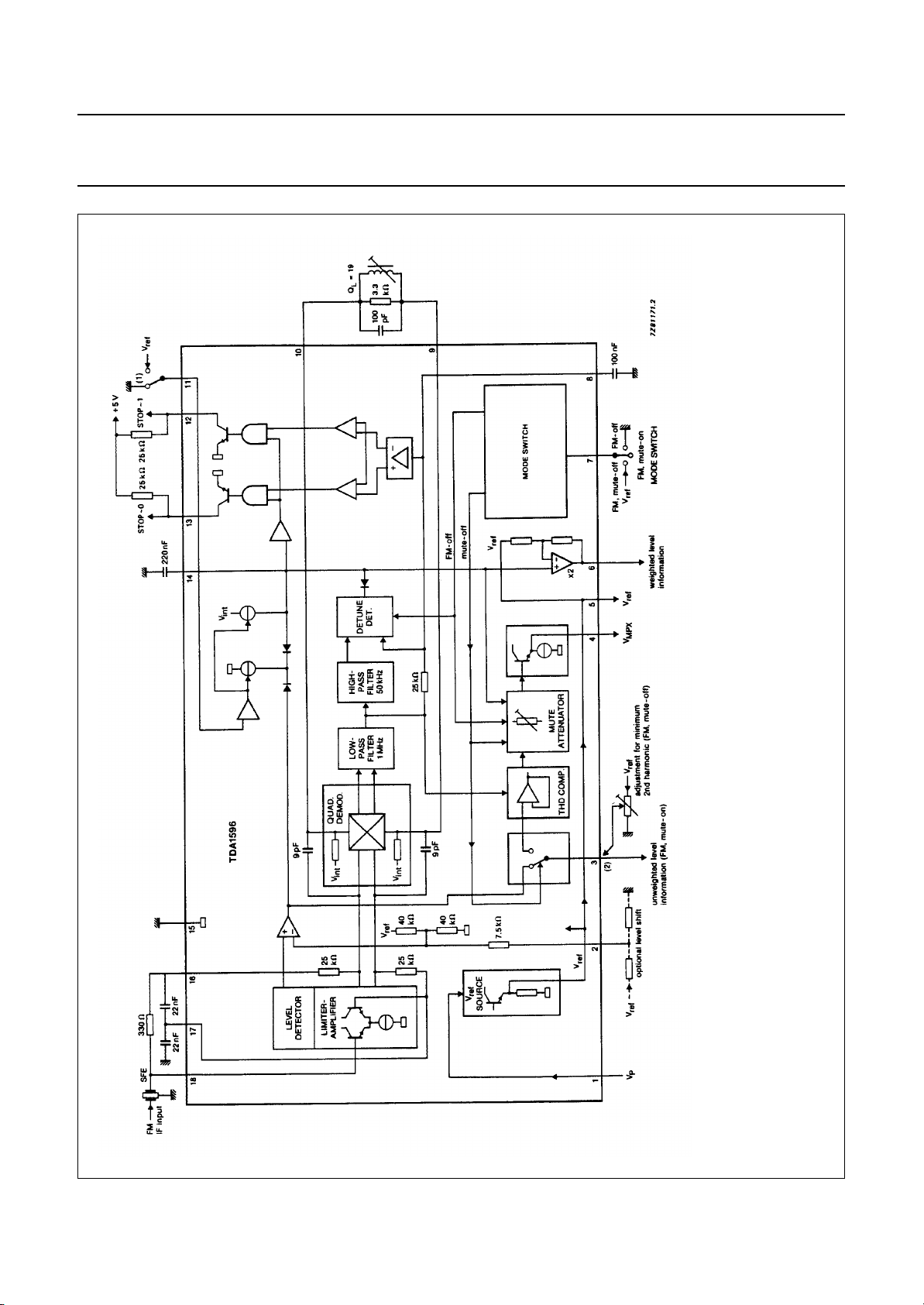
Fig.1 Block diagram and application circuit.
pin 3 can be adjusted for minimum 2nd harmonic distortion at pin 4.
(1) Connecting pin 11 to ground is only allowed for measuring the current at pin 14. It is not for use in application.
(2) In the FM, mute-on condition the unweighted level detector output is available from pin 3. In the FM, mute-off condition the variable resistor at

Philips Semiconductors Product specification
IF amplifier/demodulator for
FM radio receivers
PINNING
Fig.2 Pinning diagram.
TDA1596
1VPsupply voltage
2 LVA level voltage adjustment
3 ULV unweighted level output/K2 adjustment
4 AFO AF output
5V
6 WLV weighted level voltage output
7 MSW mode switch
8 DDV detune detector voltage
9 DMI1 demodulator input 1
10 DMI2 demodulator input 2
11 TSW tau switch
12 ST1 stop pulse output 1
13 ST0 stop pulse output 0
14 MTV mute voltage
15 GND ground
16 LFD1 IF limiter feedback 1
17 LFD2 IF limiter feedback 2
18 IFI IF input
reference voltage output
ref
April 1991 4

Philips Semiconductors Product specification
IF amplifier/demodulator for
TDA1596
FM radio receivers
FUNCTIONAL DESCRIPTION
Limiter-amplifier
This has five stages of IF amplification using balanced differential limiter-amplifiers with emitter-follower coupling.
Decoupling of the stages from the voltage supply lines and an internal high-ohmic DC feed-back loop give a very stable
IF performance. The amplifier gain is virtually independent from temperature changes.
FM demodulator
The demodulator is fully balanced and comprises two cross-coupled differential amplifiers. Quadrature detection of the
FM signal is performed by feeding one differential amplifier directly from the limiter-amplifier output, and the other via an
external 90° phase-shifting network. The demodulator has good stability and its zero cross-over shift is small.
The bandwidth of the demodulator output is restricted to approximately 1 MHz by an internal low-pass filter.
THD compensation
This circuit compensates non-linearities introduced by demodulation. For this to operate correctly the demodulator circuit
between pins 9 and 10 must have a loaded Q-factor of 19. Consequently there is no need for the demodulator tuned
circuit to be adjusted for minimum THD, instead the adjustment criterium is for a symmetrical stop pulse.
Mute attenuator and AF output
The control voltage for the mute attenuator at pin 14 is generated from the values of the level detector and the detuning
detector outputs. The mute attenuator has a fast attack and a slow decay which is determined by the capacitor at pin 14.
The AF signal is passed via the mute attenuator to the output at pin 4.
A weighted control voltage, available from pin 6, is obtained from the mute attenuator control voltage via a buffer-amplifier
which introduces an additional voltage shift and gain.
Level detector
The level detector generates a voltage output which is proportional to the field strength of the input signal.
The unweighted level detector output is available when the mode switch is operating in the FM, mute-on condition.
Tuning-stop outputs
The open collector outputs STOP-0 and STOP-1 (from pins 13 and 12 respectively) are voltages derived from the
detuning level and the field strength of the input signal. If only one tuning-stop output is required, pins 12 and 13 may be
tied together.
April 1991 5

Philips Semiconductors Product specification
IF amplifier/demodulator for
FM radio receivers
RATINGS
Limiting values in accordance with the Absolute Maximum System (IEC 134)
PARAMETER SYMBOL MIN. MAX. UNIT
Supply voltage (pin 1) V
Reference voltage range (pin 5) V
Level adjustment range (pin 2) V
Mode switch voltage range (pin 7) V
Control input voltage range (pin 11) V
THD compensation/unweighted field
strength voltage range (pin 3) V
Tuning-stop output voltage range
STOP-0 (pin 13) V
STOP-1 (pin 12) V
Tuning-stop output current
STOP-0 (pin 13) I
STOP-1 (pin 12) I
Storage temperature range T
Operating ambient temperature range T
Electrostatic handling
*
all pins except pins 5 and 6 V
pin 5 V
pin 6 V
P
5-15
2-15
7-15
11-15
3-15
13-15
12-15
13
12
stg
amb
es
es
es
= V
1-15
−0.3 + 16 V
−0.3 + 10 V
−0.3 + 10 V
−0.3 + 16 V
−0.3 + 6V
−0.3 + 16 V
−0.3 + 16 V
−0.3 + 16 V
− 2mA
− 2mA
−55 + 150 °C
−40 + 85 °C
−2000 +2000 V
−2000 +900 V
−2000 +1600 V
TDA1596
*
Equivalent to discharging a 100 pF capacitor through a 1.5 kΩ series resistor.
April 1991 6
 Loading...