

Philips TDA1592T Datasheet

INTEGRATED CIRCUITS
DATA SH EET
TDA1592
PLL stereo decoder and noise
blanker
Preliminary specification
Supersedes data of June 1993
File under Integrated Circuits, IC01
1996 May 31
Philips Semiconductors Preliminary specification
PLL stereo decoder and noise blanker TDA1592
FEATURES
• Adjustment-free voltage controlled PLL oscillator for
ceramic resonator (f = 456 kHz)
• Pilot signal dependent mono/stereo switching
• Analog control of mono/stereo change over
[stereo blend, Stereo Noise Controller (SNC)]
• Adjacent channel noise suppression (114 kHz)
• Pilot canceller
• Analog control of de-emphasis; High Cut Control (HCC)
• Reduced and controlled de-emphasis for AM operation
(pin 7 to GND)
• Applicable as source selector for AM/FM/cassette
switching
• Soft mute for silent tuning
• Separate interference noise detector
• Integrated input low-pass filter for delayed noise
blanking
• Noise blanking at MPX-demodulator outputs.
QUICK REFERENCE DATA
GENERAL DESCRIPTION
The TDA1592 is a monolithic bipolar integrated circuit
providing the stereo decoder function and noise blanking
for FM car radio applications.
The device operates in a power supply range of
7.5 to 12 V.
SYMBOL PARAMETER MIN. TYP. MAX. UNIT
V
P
I
P
V
o(rms)
supply voltage (pin 5) 7.5 10 12 V
supply current − 15 20 mA
audio output signal (RMS value) 800 900 1000 mV
THD total harmonic distortion − 0.1 0.3 %
S/N signal-to-noise ratio − 82 − dB
α
cs
V
trigg
channel separation 30 40 − dB
interference voltage trigger level − 10 − mV
ORDERING INFORMATION
TYPE
NUMBER
NAME DESCRIPTION VERSION
PACKAGE
TDA1592 DIP20 plastic dual in-line package; 20 leads (300 mil) SOT146-1
TDA1592T SO20 plastic small outline package; 20 leads; body width 7.5 mm SOT163-1
1996 May 31 2

Philips Semiconductors Preliminary specification
PLL stereo decoder and noise blanker TDA1592
BLOCK DIAGRAM
out
R
input
auxiliary
HCC
V
SNC
V
ref
andbook, full pagewidth
V
out R
R
6.8
6.8
nF
nF
11
(120 kHz)
ref
V
DETECTOR
NOISE AND AGC
AGC
kΩ
6.8
TDA1592
SNC
ref
V
AND
HCC
GATE
7.4 kΩ
7.4 kΩ
FILTER
2-POLE
(30 kHz)
MUTE
6.8 kΩ
PULSE
DETECTOR
INTERFERENCE
AMPLIFIER
HIGH-PASS
ref
V
FORMER
47 kΩ
15 14 13 12
10987654321
out L
47 kΩ
R
BC548
820
33 kΩ
47
68
pF
off
VCO
47 kΩ
27 kΩ
27 kΩ
kΩ
nF
33 pF
out
L
MED724
input
auxiliary
mute
input
interference
P
V
mono
in
R
164 kΩ
18 17 16
SWITCH
PILOT
CANCEL
19
PILOT
DETECTOR
PHASE
ref
V
20
75
kΩ
FILTER
4-POLE
(80 kHz)
pilot
indicator
MPX input
kΩ
750
100 nF
100 nF
1996 May 31 3
19 19 19 38
DETECTOR
LOGIC
ref
I
ref
V
POWER
SUPPLY
100 kΩ
100 nF
Fig.1 Block diagram with external components, also used as test circuit.
CSB
VCO
456 F11
10 nF
68 kΩ
100 nF
Philips Semiconductors Preliminary specification
PLL stereo decoder and noise blanker TDA1592
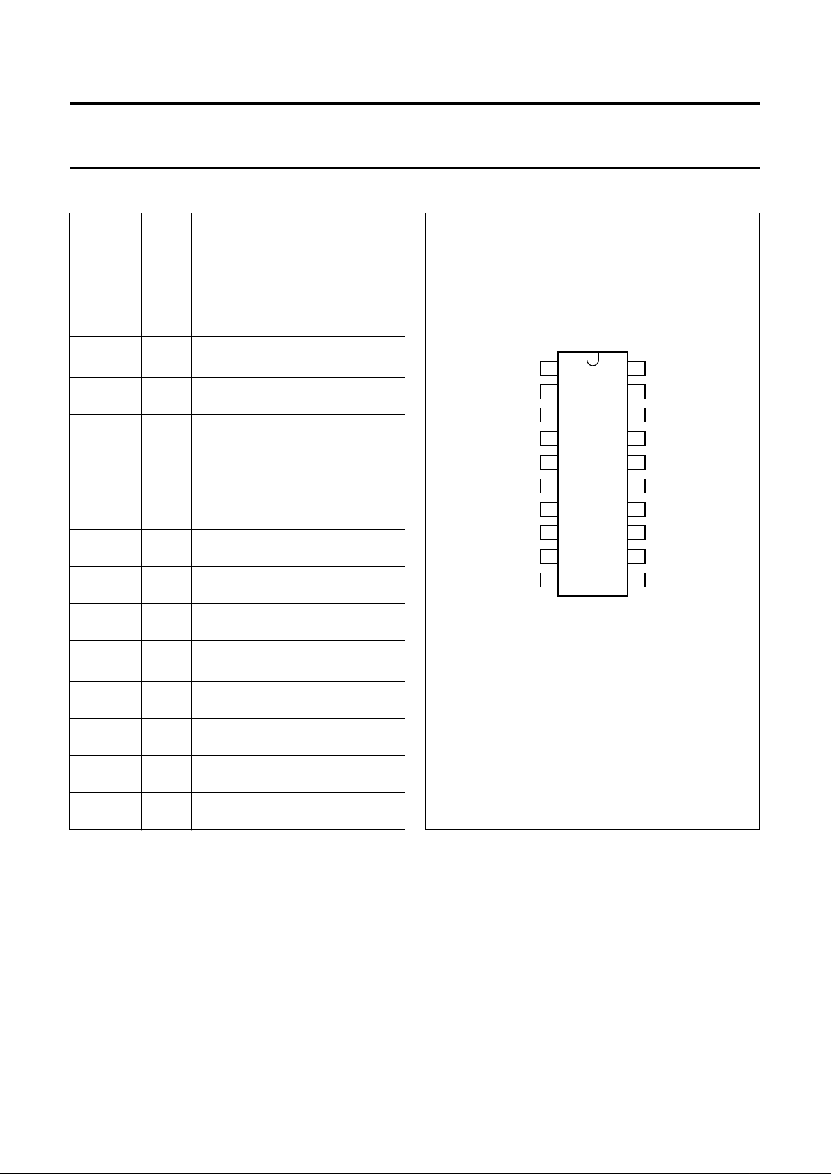
PINNING
SYMBOL PIN DESCRIPTION
PLL 1 phase locked loop filter
OSC
GND 3 ground (0 V)
I
ref
V
P
INFI 6 interference signal input
PUFO
NDET
FB-L
V
oL
V
oR
FB-R
C
DEEL
C
DEER
HCC 15 HCC input for de-emphasis control
SNC 16 stereo blend input
V
ref
IDENT
PILOT
V
i MPX
oscillator input/output pin for
2
ceramic resonator
4 reference current
5 supply voltage (+10 V)
pulse former time constant; VCO
7
off
noise detector time constant; mute
8
on
AF feedback input for left audio
9
signal
10 AF output signal left
11 AF output signal right
AF feedback input for right audio
12
signal
de-emphasis capacitor for left
13
channel
de-emphasis capacitor for right
14
channel
externally applied reference
17
voltage of 1 to 5 V
identification output (HIGH = pilot
18
existing; stereo)
pilot detector level (forced mono
19
input)
MPX input signal from IF
20
demodulator
handbook, halfpage
PLL
1
OSC
2
GND
3
I
4
ref
V
5
P
6
7
8
9
10
TDA1592
MED726
INFI
PUFO
NDET
FB-L
V
oL
Fig.2 Pin configuration.
V
20
i MPX
19
PILOT
18
IDENT
17
V
ref
16
SNC
HCC
15
C
14
DEER
C
13
DEEL
FB-R
12
V
11
oR
1996 May 31 4

Philips Semiconductors Preliminary specification
PLL stereo decoder and noise blanker TDA1592
FUNCTIONAL DESCRIPTION
The MPX input of the TDA1592 (pin 20) is the null-node of
an operational amplifier with internal feedback resistor.
Adapting the stereo decoder input to the level of the FM
demodulator output is realized by the value of input
resistor Rin (see Fig.3). The total gain of the stereo
decoder is applicable by varying the feedback resistors
R
(pins 9, 10, 11 and 12) of the output operational
out
amplifiers (see Fig.4).
The input amplifier is followed by an integrated 4th order
Bessel low-pass filter with a cut-off frequency of 80 kHz.
It provides necessary signal delay for noise blanking and
damping of high frequency interferences at the stereo
decoder input.
The soft mute facility (pin 8) provides silent tuning for RDS
processing. The mute time constant may be adjusted from
pin 8. In mute position and the VCO switched off (pin 7),
the output amplifiers can be used for cassette playback,
AM stereo purpose or other signal sources.
The voltage to current converted MPX signal is fed to
phase detector, pilot detector and pilot canceller circuits.
The oscillator is alignment-free with an external ceramic
resonator at 456 kHz as reference (pin 2). The required
19 kHz and 38 kHz signals are generated by division of the
oscillator output signal in a logical circuit. For regeneration
of the 38 kHz subcarrier, a PLL is used. The 19 kHz
quadrature phase signal is fed to the 19 kHz
phase detector, where it is compared with the incoming
pilot tone. The DC output signal of the phase detector
(pin 1) controls the oscillator (PLL).
The pilot presence detector is driven by internally
generated in-phase 19 kHz. Its pilot-dependent DC output
voltage (pin 19) is fed to a threshold switch, which
activates the pilot indicator logic output (pin 18) and turns
the stereo decoder to stereo operation. The same
DC voltage is used to control the amplitude of an
anti-phase internally generated 19 kHz signal. In the
pilot canceller, the pilot tone is compensated by this
anti-phase 19 kHz signal.
The pilot cancelled signal is fed to the multiplex decoder.
There, the side signal is demodulated and combined with
the main signal in a matrix to left and right audio channel.
Compensation for roll-off in the incoming MPX signal
caused by IF filters and FM demodulator is realized by
corresponding side signal amplification.
A smooth mono to stereo take-over, which is controlled by
the level detector voltage of the IF part, is achieved by the
SNC (pins 16 and 17; see Fig.6).
From the output of the MPX demodulator the signals are
fed to 2-pole low-pass filters with a cut-off frequency of
30 kHz to provide additional signal delay for noise blanking
and attenuation of the subcarrier and its harmonics.
These filters are followed by the noise suppression gates,
which are combined with de-emphasis and HCC. The
de-emphasis is defined by internal resistors (aligned by an
external current) and external capacitors (pins 13 and 14).
For HCC, the de-emphasis time constant can be changed
to higher values (pins 15 and 17; see Figs 7 to 9). This
function is controlled by an analog input signal, derived
from the level detector voltage of the IF part. When the
VCO is turned off (pin 7 to GND), de-emphasis is reduced
to 20 µs for full frequency response when AM-AF is fed
through the stereo decoder. De-emphasis remains
controllable.
From the gate circuits audio is fed through internal series
resistors to the inverting inputs of the output operational
amplifiers (pins 9 and 12), which can also be used as
signal inputs for cassette playback or other sources when
the mute is activated. The gain of these amplifiers is
defined by external feedback resistors R
(pins 9, 10, 11 and 12).
The input of the ignition noise blanker is the null node of an
operational amplifier (pin 6). It can be driven by the level
detector output of the FM-IF limiter and/or the MPX signal.
Its sensitivity is dependent on the value of the series input
resistor at pin 6.
The operational amplifier output signal is fed through an
integrated 120 kHz high-pass filter, becomes amplified
and is then fed in parallel to the noise detector and the
interference detector. The noise detector is a negative
peak detector. Its output (pin 8) controls the trigger
sensitivity (prevention to false triggering at noisy input
signals) and the attenuation of the input operational
amplifier. The output of the interference detector, when
receiving a steep pulse, triggers a mono flip-flop, which is
a part of the pulse former circuit. The time constant of the
mono flip-flop is defined by an external capacitor (pin 7)
and its output activates the blanking gates in the audio.
out
1996 May 31 5
Philips Semiconductors Preliminary specification
PLL stereo decoder and noise blanker TDA1592
LIMITING VALUES
In accordance with the Absolute Maximum Rating System (IEC 134).
SYMBOL PARAMETER MIN. MAX. UNIT
V
P
P
tot
T
stg
T
amb
V
es
Note
1. Equivalent to discharging a 200 pF capacitor through a 0 Ω series resistor.
CHARACTERISTICS
= 10 V; T
V
P
amb
and series resistor at input R1= 164 kΩ; measurements taken in Fig.1; unless otherwise specified.
supply voltage (pin 5) 0 13.2 V
total power dissipation 0 0.25 W
storage temperature −55 +150 °C
operating ambient temperature −40 +85 °C
electrostatic handling for all pins; note 1 −400 +400 V
=25°C; input signal V
i MPX(p-p)
= 1.7 V; m = 100% (∆f=±75 kHz, f
= 1 kHz); de-emphasis of 50 µs
mod
SYMBOL PARAMETER CONDITIONS MIN. TYP. MAX. UNIT
V
P
I
P
supply voltage (pin 5) 7.5 10 12 V
supply current − 15 20 mA
Stereo decoder
V
i MPX(p-p)
∆V
i MPX(p-p)
V
o(rms)
MPX input signal − 1.7 − V
overdrive margin of MPX input signal THD = 1% 6 −−dB
AF mono output signal at pins 10 and 11
without pilot 800 900 1000 mV
(RMS value)
∆V
o
V
10-11/Vo
V
o 10,11
R
o 10,11
I
o
R
2,3
V
4,3
α
cs
overdrive margin of output signal THD = 1% 6 −−dB
difference of output voltage levels −−1dB
DC output voltage (pins 10 and 11) 3.2 3.7 4.2 V
output resistance − 150 −Ω
output current 330 400 −µA
maximum feedback resistor −−68 kΩ
reference voltage 3.7 3.8 3.9 V
channel separation pin 16 open-circuit;
30 40 − dB
see Fig.6
THD total harmonic distortion − 0.1 0.3 %
S/N signal-to-noise ratio f = 20 to 16000 Hz 77 82 − dB
α
19
α
38
α
57
α
76
IM2 intermodulation for f
IM3 f
α
57 VF
α
67
pilot signal suppression f = 19 kHz 40 50 − dB
subcarrier suppression f = 38 kHz 35 50 − dB
f = 57 kHz 46 −−dB
f = 76 kHz − 60 − dB
= 1 kHz f
spur
= 10 kHz; note 1 − 60 − dB
mod
= 13 kHz − 58 − dB
mod
traffic radio (VWF) f = 57 kHz; note 2 − 70 − dB
SCA (Subsidiary Communications
f = 67 kHz; note 3 70 −−dB
Authorization)
1996 May 31 6
 Loading...