


DATA SH EET
Product specification
Supersedes data of March 1992
File under Integrated Circuits, IC01
1996 Sep 02
INTEGRATED CIRCUITS
TDA1591
PLL stereo decoder and noise
blanker
1996 Sep 02 2
Philips Semiconductors Product specification
PLL stereo decoder and noise blanker TDA1591
FEATURES
• Adjustment-free voltage controlled PLL oscillator for
ceramic resonator (f = 456 kHz)
• Pilot signal dependent mono/stereo switching
• Analog control of mono/stereo change over
[stereo blend, Stereo Noise Controller (SNC)]
• Adjacent channel noise suppression (114 kHz)
• Pilot canceller
• Analog control of de-emphasis; High Cut Control (HCC)
• Applicable as source selector for AM/FM/cassette
switching
• Separate interference noise detector
• Integrated input low-pass filter for delayed noise
blanking
• Noise blanking at MPX-demodulator outputs
• Internal voltage stabilization.
GENERAL DESCRIPTION
The TDA1591 is a monolithic bipolar integrated circuit
providing the stereo decoder function and noise blanking
for FM car radio applications.
The device operates in a power supply range of
7.5 to 12 V.
QUICK REFERENCE DATA
ORDERING INFORMATION
SYMBOL PARAMETER MIN. TYP. MAX. UNIT
V
P
supply voltage (pin 5) 7.5 10 12 V
I
P
supply current − 12 − mA
V
o(rms)
audio output signal (RMS value) − 900 − mV
THD total harmonic distortion − 0.1 0.3 %
S/N signal-to-noise ratio − 76 − dB
α
cs
channel separation − 40 − dB
V
trigg
interference voltage trigger level − 10 − mV
TYPE
NUMBER
PACKAGE
NAME DESCRIPTION VERSION
TDA1591 DIP20 plastic dual in-line package; 20 leads (300 mil) SOT146-1
TDA1591T SO20 plastic small outline package; 20 leads; body width 7.5 mm SOT163-1
1996 Sep 02 3
Philips Semiconductors Product specification
PLL stereo decoder and noise blanker TDA1591
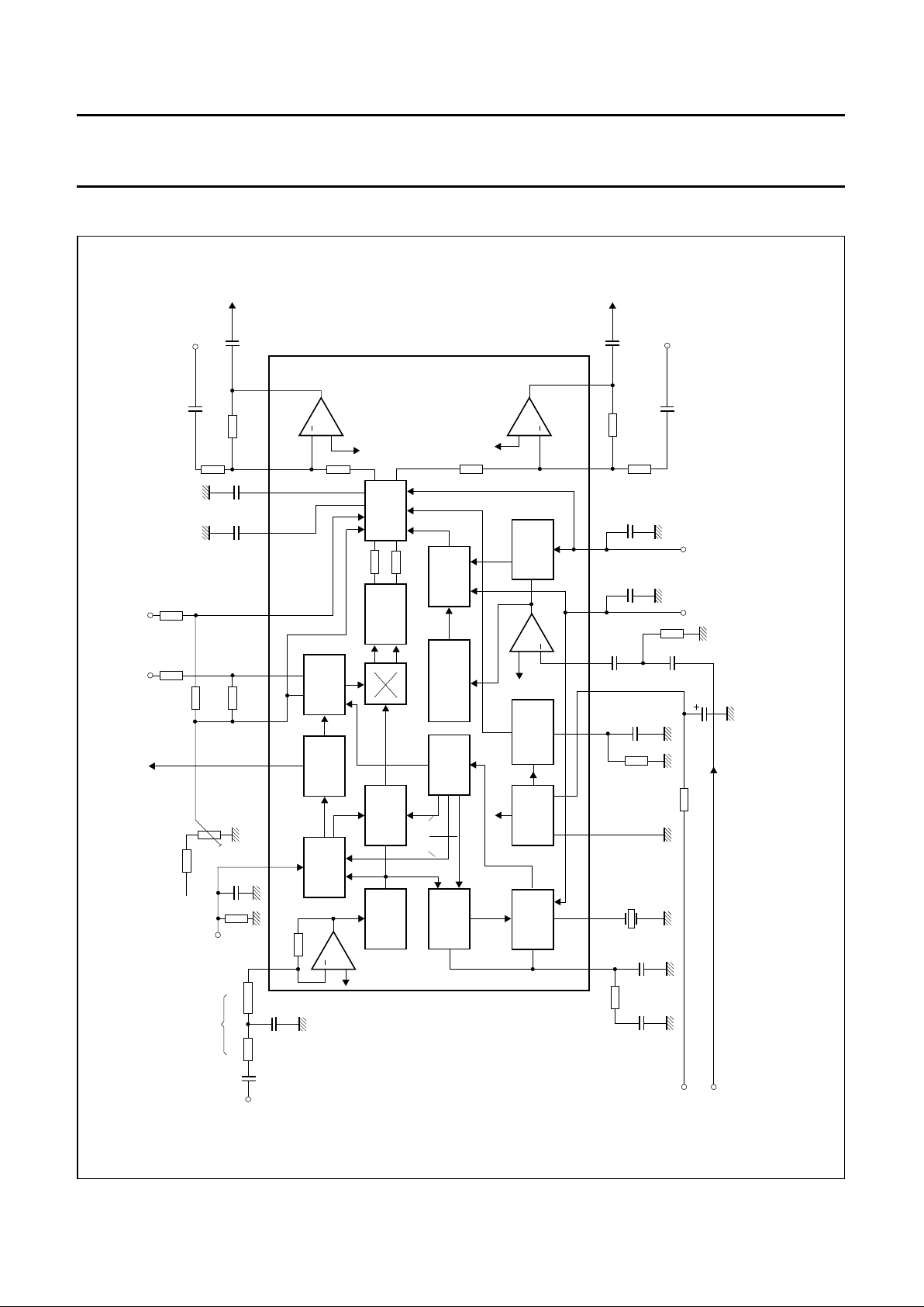
BLOCK DIAGRAM
handbook, full pagewidth
stereo
indication
SNC
HCC
V
i MPX
68 kΩ 82 kΩ
0.1 µF
68 pF
C
comp
470 kΩ
0.1
µF
10 kΩ
V
ref
= 1 to 5 V
from pin 5
27 kΩ
27 kΩ
from IF level detector
100 kΩ 100 kΩ
12 3 4567 8 9 10
111213141516
20 19 18 17
+
+
+
+
6.8 nF
6.8 nF
47 kΩ
0.22 µF
0.22 µF
V
0.22 µF
47 kΩ
47 kΩ
47 kΩ
0.22 µF
mute on
VCO off
6.5 kΩ
6.5
kΩ
PILOT
DETECTOR
SWITCH
STEREO
BLEND
4-POLE
FILTER
(80 kHz)
PILOT
CANCEL
2-POLE
FILTER
(30 kHz)
GATE
AND
HCC
PHASE
DETECTOR
LOGIC
INTERFERENCE
DETECTOR
PULSE
FORMER
VCO
VOLTAGE
STABILIZER
REFERENCE
CURRENT
NOISE
DETECTOR
470
pF
2.2
kΩ
470
pF
1.2
nF
0.1
µF
100 kΩ
CSB456F11
(Murata)
22
nF
0.22
µF
27 kΩ
V
P
= 10 V
INFI
interference signal (TDA1596, pin 3)
19 kHz
TDA1591
R1
75 kΩ
forced
mono
7.4 kΩ
7.4 kΩ
47
nF
IDENT
38 kHz
100
µF
FB-R
R2
R3
FB-L
10 Ω
(1)
MEH027
iAUX
V
oL
V
oR
V
iAUX
PILOT
12 kΩ
Fig.1 Block diagram with external components, also used as test circuit.
(1) Simulates the roll-off of the FM demodulator.
1996 Sep 02 4
Philips Semiconductors Product specification
PLL stereo decoder and noise blanker TDA1591
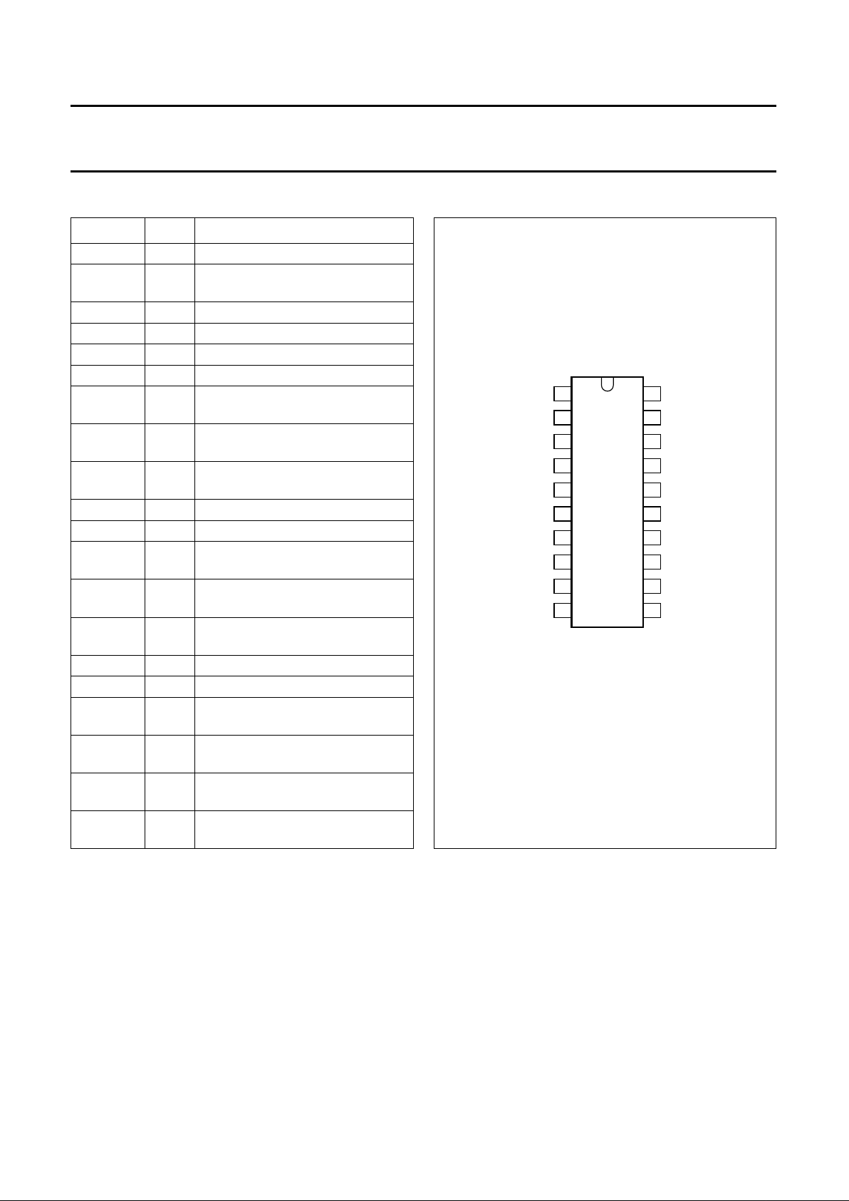
PINNING
SYMBOL PIN DESCRIPTION
PLL 1 phase locked loop filter
OSC 2 oscillator input/output pin for
ceramic resonator
GND 3 ground (0 V)
I
ref
4 reference current
V
P
5 supply voltage (+10 V)
INFI 6 interference signal input
PUFO 7 pulse former time constant;
VCO off
NDET 8 noise detector time constant;
mute on
FB-L 9 AF feedback input for left audio
signal
V
oL
10 AF output signal left
V
oR
11 AF output signal right
FB-R 12 AF feedback input for right audio
signal
C
DEEL
13 de-emphasis capacitor for left
channel
C
DEER
14 de-emphasis capacitor for right
channel
HCC 15 HCC input for de-emphasis control
SNC 16 stereo blend input
V
ref
17 externally applied reference
voltage of 1 to 5 V
IDENT 18 identification output (HIGH = pilot
existing; stereo)
PILOT 19 pilot detector level (forced mono
input)
V
i MPX
20 MPX input signal from IF
demodulator
Fig.2 Pin configuration.
handbook, halfpage
TDA1591
MHA363
1
2
3
4
5
6
7
8
9
10
20
19
18
17
16
15
14
13
12
11
PLL
OSC
GND
INFI
PUFO
NDET
FB-L
V
oL
I
ref
V
P
V
i MPX
V
oR
C
DEEL
C
DEER
HCC
SNC
IDENT
PILOT
V
ref
FB-R

1996 Sep 02 5
Philips Semiconductors Product specification
PLL stereo decoder and noise blanker TDA1591
FUNCTIONAL DESCRIPTION
Adapting the MPX input to the level of the FM demodulator
output is realized by the value of input resistor R1
(see Fig.3). The total gain of the stereo decoder is
applicable by varying the feedback resistors R2 and R3
(see Figs 1 and 4).
In mute position and the VCO switched off (pin 7), the
output amplifiers can be used for cassette playback,
AM stereo purpose or other signal sources.
The Stereo Noise Controller (SNC) provides a smooth
mono to stereo take-over (see Fig.5).
For High Cut Control (HCC), the de-emphasis time
constant can be changed to higher values
(see Figs 7 and 8). This function is controlled by an analog
input signal.
The noise blanking facility is achieved by gating the stereo
decoder output signal.
The interference detector generates a gating pulse
preferable forced by the level detector voltage of the IF
part.
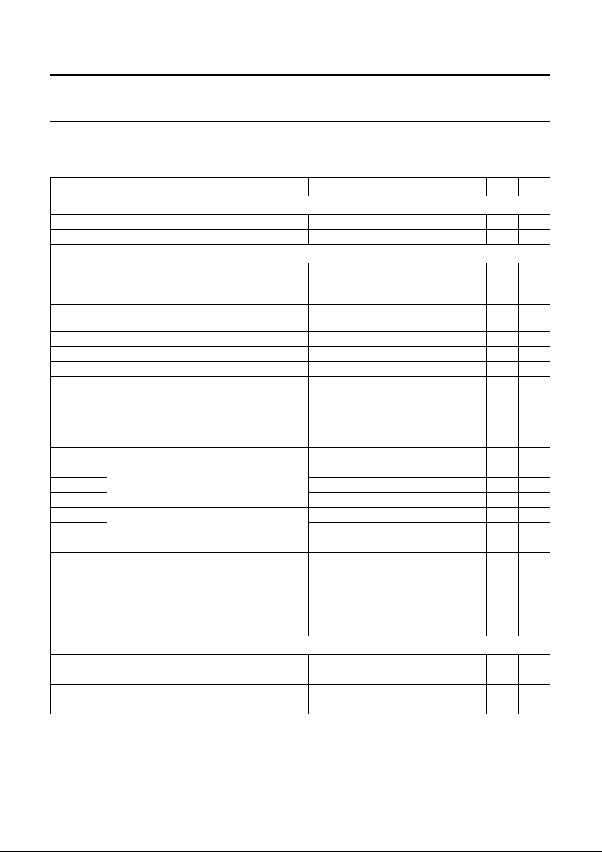
LIMITING VALUES
In accordance with the Absolute Maximum Rating System (IEC 134).
Note
1. Equivalent to discharging a 200 pF capacitor through a 0 Ω series resistor.
SYMBOL PARAMETER MIN. MAX. UNIT
V
P
supply voltage (pin 5) 0 13.2 V
P
tot
total power dissipation 0 0.25 W
T
stg
storage temperature −55 +150 °C
T
amb
operating ambient temperature −40 +85 °C
V
es
electrostatic handling; note 1
pins 1 and 16 −400 +400 V
pin 5 −300 +300 V
all other pins −600 +600 V
1996 Sep 02 6
Philips Semiconductors Product specification
PLL stereo decoder and noise blanker TDA1591
CHARACTERISTICS
VP= 10 V; T
amb
=25°C; input signal V
i MPX(p-p)
= 1.7 V; m = 100% (∆f=±75 kHz, f
mod
= 1 kHz); de-emphasis of 50 µs
and series resistor at input R1 = 150 kΩ; measurements taken in Fig.1; unless otherwise specified.
SYMBOL PARAMETER CONDITIONS MIN. TYP. MAX. UNIT
Supply
V
P
supply voltage (pin 5) 7.5 10 12 V
I
P
supply current − 12 − mA
Stereo decoder
V
i MPX(p-p)
MPX input signal on pin 20
(peak-to-peak value)
− 1.7 − V
∆V
i MPX(p-p)
overdrive margin of MPX input signal THD = 1% 3 −−dB
V
o(rms)
AF mono output signal at pins 10 and 11
(RMS value)
without pilot − 900 − mV
∆V
o
overdrive margin of output signal THD = 1% 3 −−dB
V
10-11/Vo
difference of output voltage levels −−1dB
V
o 10,11
DC output voltage (pins 10 and 11) 3.3 3.8 4.3 V
R
o 10,11
output resistance − 130 −Ω
α
cs
channel separation pin 16 open-circuit;
see Fig.6
− 40 − dB
THD total harmonic distortion − 0.1 0.3 %
S/N signal-to-noise ratio f = 20 to 16000 Hz − 76 − dB
α
19
pilot signal suppression f = 19 kHz − 50 − dB
α
38
subcarrier suppression f = 38 kHz − 50 − dB
α
57
f = 57 kHz − 46 − dB
α
76
f = 76 kHz − 60 − dB
IM2 intermodulation for f
spur
= 1 kHz f
mod
= 10 kHz; note 1 − 60 − dB
IM3 f
mod
= 13 kHz; note 1 − 58 − dB
α
57
ARI traffic radio (ARI) f = 57 kHz; note 2 − 70 − dB
α
67
Subsidiary Communication Authorization
(SCA)
f = 67 kHz; note 3 70 −−dB
α
114
Adjacent Channel Interference (ACI) f = 114 kHz; note 4 − 80 − dB
α
190
f = 190 kHz; note 4 − 70 − dB
PSRR power supply ripple rejection f = 100 Hz;
V
ripple(rms)
= 100 mV
− 35 − dB
VCO (pin 2)
f
osc
oscillator frequency (ceramic resonator) − 456 − kHz
frequency range of free running oscillator 452 − 460 kHz
∆f/f capture and holding range − 1 − %
V
7
VCO-off voltage (pin 7) 0 − 0.6 V
 Loading...