

Philips tda1581t DATASHEETS

INTEGRATED CIRCUITS
DATA SH EET
TDA1581T
Decoder for traffic warning (VWF)
radio transmissions
Preliminary specification
File under Integrated Circuits, IC01
March 1992

Philips Semiconductors Preliminary specification
Decoder for traffic warning (VWF) radio
TDA1581T
transmissions
FEATURES
• Selective subcarrier amplifier (57 kHz) with gain control
• Transmitter identification signal (SK) decoder
• Area identification signal (BK) and announcement
identification signal (DK) active filtering
• BK and DK decoders (Schmitt trigger with switched
hysteresis)
• BK and DK switch-on/switch-off delay circuits
• SK and BK control outputs.
QUICK REFERENCE DATA
Measured in Fig.3 at V
C’ signal; or with f
m
= 8 mV; f = 57 kHz amplitude modulated with fm = 34.95 Hz and m = 60% for ‘BK-traffic area
iSK
= 125 Hz and m = 30% for DK signal
SYMBOL PARAMETER CONDITIONS MIN. TYP. MAX. UNIT
V
P
I
P
V
iSK
Z
i
V
iSK
V
i(p-p)
m
BKon
∆m
BK
t
dSKon
t
dSKoff
m
DKon
∆m
DK
t
dDKon
t
dDKoff
T
amb
supply voltage range 7.5 8.5 10 V
supply current − 6 − mA
nominal input voltage f = 57 kHz − 8 − mV
input impedance f ≤ 57 kHz 100 −−kΩ
control level −3 dB − 2.4 − mV
input voltage peak-to-peak value 2 −−V
SK switch-on threshold level − 42 − %
SK switch hysteresis − 3.5 − dB
SK switch-on delay − 150 − ms
SK switch-off delay − 750 − ms
DK switch-on threshold level − 13 − %
DK switch hysteresis − 3.6 − dB
DK switch-on delay − 750 − ms
DK switch-off delay − 750 − ms
operating ambient temperature range −30 − +80 °C
GENERAL DESCRIPTION
The TDA1581T decoder is for radio transmissions having
57 kHz amplitude-modulated subcarriers as used in the
german ‘Verkehrs Warnfunk’ (VWF) traffic warning
system.
ORDERING INFORMATION
PACKAGE
EXTENDED
TYPE NUMBER
PINS PIN POSITION MATERIAL CODE
TDA1581T 20 SO plastic SOT163A
Note
1. SOT163-1; 1996 August 28.
March 1992 2
(1)
Philips Semiconductors Preliminary specification
Decoder for traffic warning (VWF) radio
transmissions
TDA1581T
March 1992 3
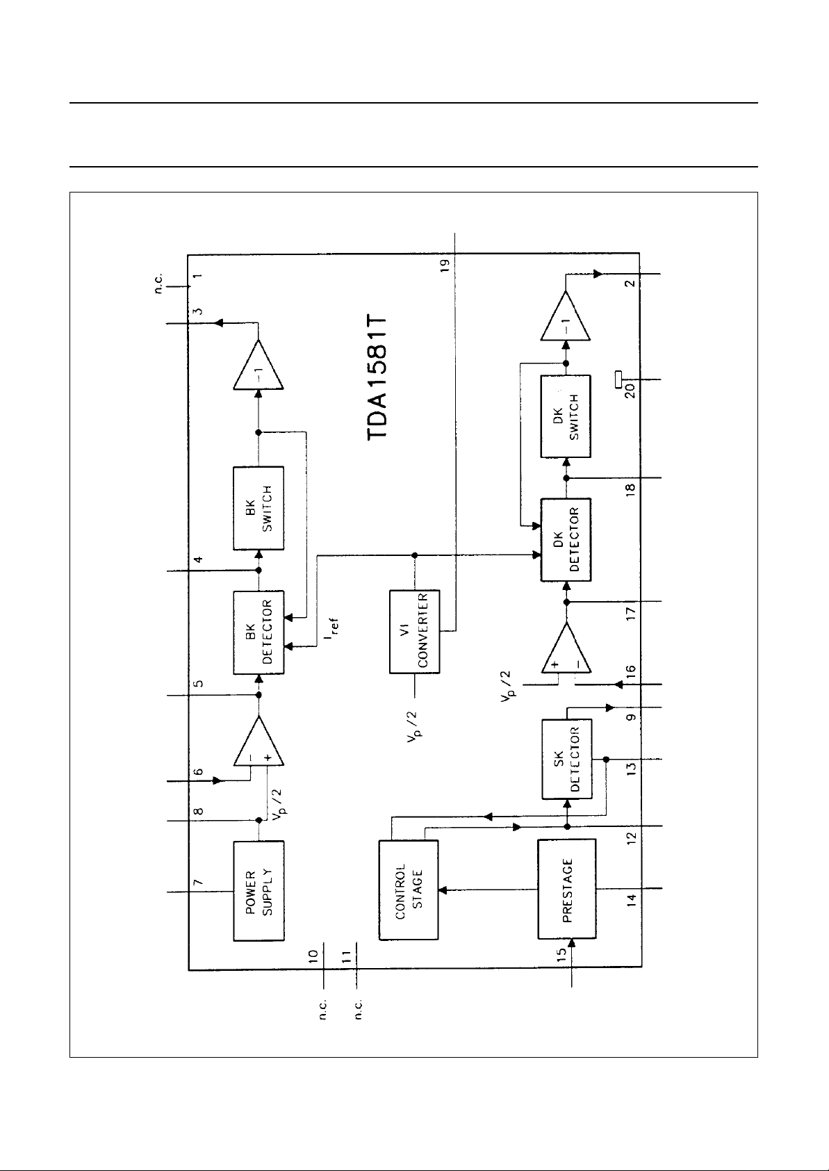
Fig.1 Block diagram.
Philips Semiconductors Preliminary specification
Decoder for traffic warning (VWF) radio
transmissions
PINNING
SYMBOL PIN DESCRIPTION
n.c. 1 not connected
DK
out
SK
out
τ
BK
V
5BK
V
6BK
V
P
/ 2 8 half supply voltage
V
P
V
9SK
n.c. 10 not connected
n.c. 11 not connected
V
12SK
V
AGC
I
14
V
MPX
V
16DK
V
17DK
τ
DK
I
19
GND 20 ground
2 DK output current
3 SK output current
4 time delay BK
5 filter output BK
6 filter input BK
7 supply voltage
9 SK detector output
12 57 kHz band pass filter
13 AGC
14 prestage biasing current
15 MPX input
16 filter input DK
17 filter output DK
18 time delay DK
19 reference current for BK, DK detector
TDA1581T
Fig.2 Pin configuration.
March 1992 4

Philips Semiconductors Preliminary specification
Decoder for traffic warning (VWF) radio
TDA1581T
transmissions
LIMITING VALUES
In accordance with the Absolute Maximum System (IEC134).
SYMBOL PARAMETER CONDITIONS MIN. TYP. MAX. UNIT
= V
V
P
7-20
V
2; 3-20
I
2; 3
V
15-20
I
15
P
tot
T
stg
T
amb
CHARACTERISTICS
= 8.5 V; T
V
p
= 34.95 Hz and m = 60% for ‘BK-traffic area C’ signal; or with fm = 125 Hz and m = 30% for DK signal.
f
m
SYMBOL PARAMETER CONDITIONS MIN. TYP. MAX. UNIT
V
P
I
P
SK amplifier/decoder
Z
i
V
i(p-p)
V
iSK
G
v9-15
∆G
v9-15
∆G
v
V
o9BK
V
o9DK
BK circuit
V
o5BKon
V
o5BKon
--------------------- V
o5BKoff
V
4-20off
I
3
V
3-20sat
V
3-20
supply voltage pin 7 −−15 V
switch output voltage pins 2 or 3 −0.5 − 15 V
switch output current pins 2 or 3 −10 − 5mA
signal input voltage pin 15 −0.5 − V
P
signal input current pin 15 −−−10 mA
total power dissipation −−800 mW
storage temperature range −55 − +150 °C
operating ambient temperature range −30 − +80 °C
= +25 °C; measured at nominal input signal: V
amb
= 8 mV, f = 57 kHz amplitude modulated with
iSK
supply voltage pin 7 7.5 − 10 V
supply current pin 7 − 615mA
input impedance f ≤ 57 kHz 60 −−kΩ
input voltage (peak-to-peak value) 2 −−V
input voltage at start of gain control V
voltage gain V
= −3 dB − 2.4
o9BK
9BK
/ V
15SK
− 44
(1)
(1)
− mV
− dB
gain spread −−±2dB
gain control range 40 −−dB
controlled output voltage − 440 − mV
− 220 − mV
switch-on threshold level pin 3 high-Z 600 670 750 mV
switch hysteresis 3 3.5 4 dB
BK switch threshold level for BK-off
(SK-off) (typ. value = 0.21V
8-20
)
pin 3 conducting 0.8 0.88 0.97 V
SK output (pin 3)
permitted load current −−0.5 mA
saturation voltage I3 = 1.5 mA −−0.35 V
rejection voltage I3<5µA18−−V
V
March 1992 5
 Loading...