


INTEGRATED CIRCUITS
DATA SH EET
TDA1575T
FM front end circuit for CENELEC
EN 55020 applications
Preliminary specification
File under Integrated Circuits, IC01
April 1993

Philips Semiconductors Preliminary specification
FM front end circuit for CENELEC EN
TDA1575T
55020 applications
FEATURES
• Bipolar integrated FM front end circuit, designed for use
in car radios and home receivers
• Fulfills CENELEC EN 55020 requirements
• Radio frequency range of 76 to 90 MHz (Japan) or 87.5
to 108 MHz (Europe, USA)
• Low noise oscillator, buffered oscillator output
• Double balanced mixer
• Internal buffered mixer driving
• Linear IF amplifier, suitable for ceramic IF filters
• Regulated reference voltage.
QUICK REFERENCE DATA
SYMBOL PARAMETER MIN. TYP. MAX. UNIT
V
P
I
P
V
REF
Z
I
NF noise figure of mixer − 9 − dB
EMF1 3rd order intermodulation − 115 − dBµV
V
OSC
THD total harmonic distortion −−15 − dBC
G
v
NF IF noise figure − 6.5 − dB
Z
I
Z
O
EMF2 AGC wideband threshold (RMS value) − 17 − mV
supply voltage 7 8.5 10 V
supply current, without mixer − 23 − mA
reference voltage output − 4.2 − V
mixer input impedance − 14 −Ω
oscillator buffer output signal (RMS value) 75 −−mV
IF gain − 30 − dB
IF input impedance − 300 −Ω
IF output impedance − 300 −Ω
ORDERING INFORMATION
EXTENDED
TYPE NUMBER
TDA1575T 16 mini-pack plastic SOT109A
Note
1. SOT109-1; 1996 August 29.
April 1993 2
PACKAGE
PINS PIN POSITION MATERIAL CODE
(1)
Philips Semiconductors Preliminary specification
FM front end circuit for CENELEC EN
55020 applications
TDA1575T
Coils TOKO
L1: MC-108 514 HNE-150023S14; L = 78 nH, N = 4 turns
L2: MC-111 E516 HNS-200057; L = 80 nH
L3: A119 ACS-17114 FTT
April 1993 3
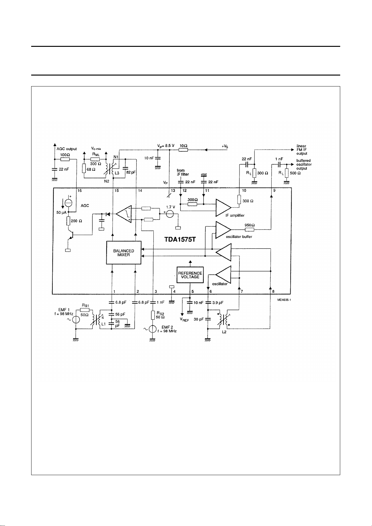
Fig.1 Block diagram and test circuit.
Philips Semiconductors Preliminary specification
FM front end circuit for CENELEC EN
55020 applications
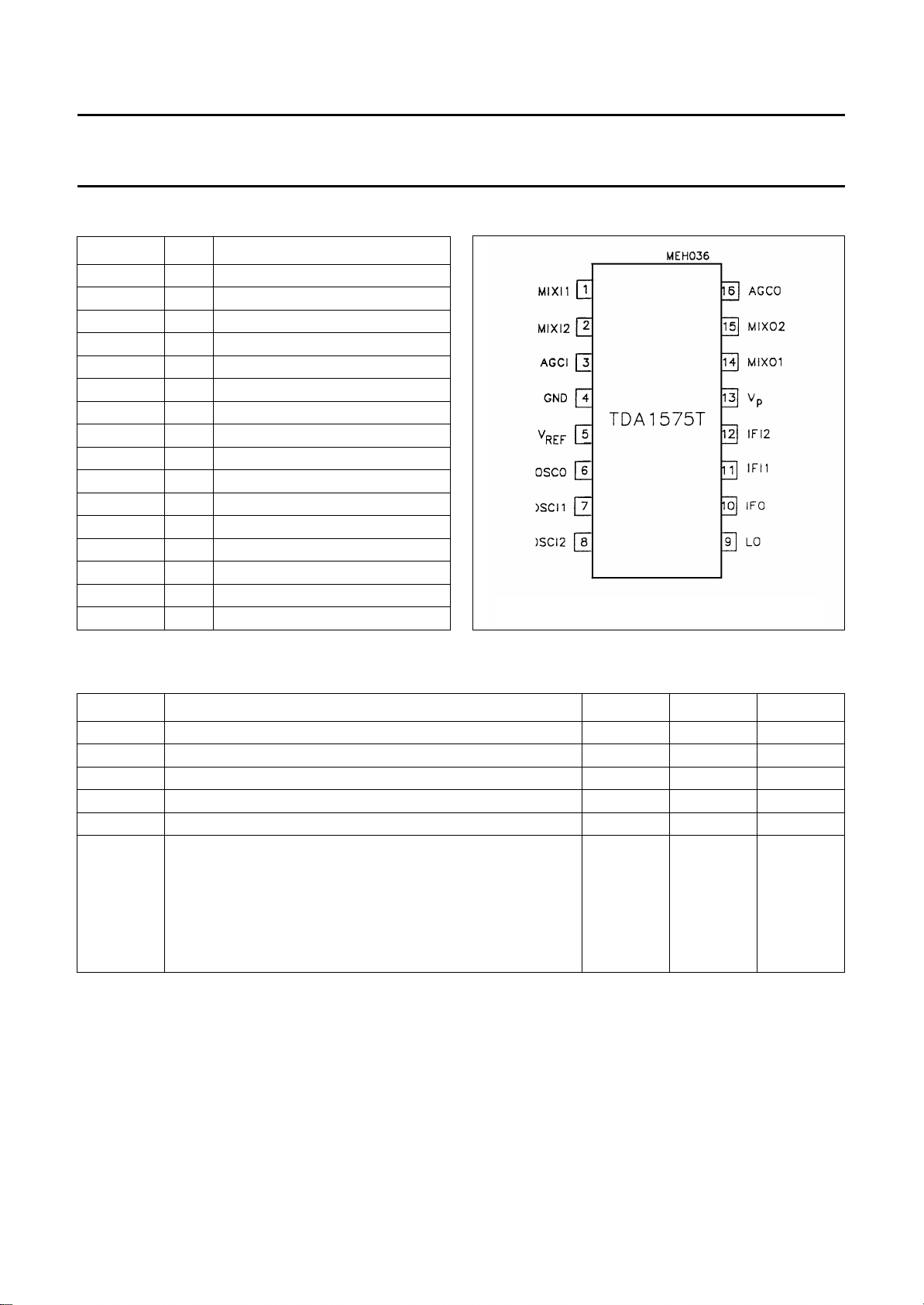
PINNING
SYMBOL PIN DESCRIPTION
MIXI1 1 RF input 1 to mixer
MIXI2 2 RF input 2 to mixer
AGCI 3 HF input to automatic gain control
GND 4 ground (0 V)
V
REF
OSCO 6 oscillator output
OSCI1 7 oscillator input 1
OSCI2 8 oscillator input 2
LO 9 buffered oscillator output
IFO 10 linear FM IF output
IFI1 11 FM IF input 1
IFI2 12 FM IF input 2
V
P
MIXO1 14 mixer output 1
MIXO2 15 mixer output 2
AGCO 16 automatic gain control output
5 reference voltage output
13 supply voltage (+8.5 V)
TDA1575T
Fig.2 Pin configuration.
LIMITING VALUES
Limiting values in accordance with the Absolute Maximum System (IEC 134).
SYMBOL PARAMETER MIN. MAX. UNIT
V
V
P
T
T
V
P
14, 15
tot
stg
amb
ESD
supply voltage (pin 13) 0 12 V
voltage at mixer output 0 V
P
V
total power dissipation 0 380 mW
storage temperature range −55 +150 °C
operating ambient temperature range −40 +85 °C
electrostatic handling (see note 1)
all pins except 3 and 10 −±2000 V
pin 3 − +2000 V
−−1000 V
pin 10 − +1500 V
−−2000 V
Note to the limiting values
1. Equivalent to discharging a 100 pF capacitor through a 1.5 kΩ series resistor.
April 1993 4

Philips Semiconductors Preliminary specification
FM front end circuit for CENELEC EN
TDA1575T
55020 applications
CHARACTERISTICS
= 8.5 V and T
V
P
SYMBOL PARAMETER CONDITIONS MIN. TYP. MAX. UNIT
V
P
I
P
V
REF
Mixer; EMF1 = 98 MHz
I
14 + 15
V
1, 2
Z
1, 2
V
14, 15
C
14, 15
G
P
EMF1
IP3
NF noise figure − 9 − dB
= +25°C, measurements taken in Fig.1 with f0 = 98 MHz (EMF1) unless otherwise specified.
amb
supply voltage (pin 13) 7 8.5 10 V
supply current without mixer 16 23 30 mA
reference voltage (pin 5) I5 ≤ 3 mA 3.9 4.2 4.4 V
mixer supply current (pins 14 and 15) − 4 − mA
DC voltage input (pins 1 and 2) − 1 − V
input impedance − 14 −Ω
DC output voltage (pins 14 and 15) 4 − 10 V
output capacitance − 13 − pF
conversion power gain note 1 − 14 − dB
3rd order intercept point − 115 − dBµV
total noise figure including
− 11 − dB
transforming network
Oscillator; f
V
7, 8
V
6
∆f residual FM at pin 6 f = 300 to 15000 Hz;
= 108.7 MHz
OSC
DC input voltage (pins 7 and 8) − 1.3 − V
DC output voltage (pin 6) − 2.0 − V
− 2.2 − Hz
de-emphasis 50 µs
Oscillator buffered output (pin 9)
V
O
V
9
R
9
output signal (RMS value) RL= 500 Ω; CL= 2 pF 75 −−mV
DC output voltage − 6 − V
DC output resistor − 950 −Ω
THD total harmonic distortion −−15 − dBC
f
S
spurious frequencies EMF1 = 2 V;
−−37 − dBC
RS= 50 Ω;
f
= 108.7 MHz
OSC
Automatic gain control (AGC); f
R
3
C
3
V
16
I
16
input resistance (pin 3) − 4 − kΩ
input capacitance − 3 − pF
AGC output swing (DC) Figs 3 and 4 0.5 − VP − 0.3 V
output current at I3 = 0 V16 = 1/2 V
output current at U
EMF2 threshold (RMS value) I
= 98 MHz
i
P
= 2 V V16 = 7 to 10 V 2 − 5mA
3
= 0; V16 = 1/2 VP;
16
−25 −50 −150 µA
− 17 − mV
Figs 4 and 5
April 1993 5
 Loading...