

Philips TDA1563Q-N1-S400, TDA1563Q-N1 Datasheet

DATA SH EET
Product specification
Supersedes data of 1998 Jul 14
File under Integrated Circuits, IC01
2000 Feb 09
INTEGRATED CIRCUITS
TDA1563Q
2 × 25 W high efficiency car radio
power amplifier

2000 Feb 09 2
Philips Semiconductors Product specification
2 × 25 W high efficiency car radio power
amplifier
TDA1563Q
FEATURES
• Low dissipation due to switching from Single-Ended
(SE) to Bridge-Tied Load (BTL) mode
• Differential inputs with high Common Mode Rejection
Ratio (CMRR)
• Mute/standby/operating (mode select pin)
• Zero crossing mute circuit
• Load dump protection circuit
• Short-circuit safe to ground, to supply voltage and
across load
• Loudspeaker protection circuit
• Device switches to SE operation at excessive junction
temperatures
• Thermal protectionat high junction temperature (170°C)
• Diagnostic information (clip detection and
protection/temperature)
• Clipping information can be selected between
THD = 2.5% or 10%
GENERAL DESCRIPTION
The TDA1563Q is a monolithic power amplifier in a
17-lead DIL-bent-SIL plastic power package. It contains
two identical 25 W amplifiers. The dissipation is minimized
by switching from SE to BTL mode when a higher output
voltage swing is needed. The device is primarily
developed for car radio applications.
QUICK REFERENCE DATA
ORDERING INFORMATION
SYMBOL PARAMETER CONDITIONS MIN. TYP. MAX. UNIT
V
P
supply voltage DC biased 6 14.4 18 V
non-operating −−30 V
load dump −−45 V
I
ORM
repetitive peak output current −−4A
I
q(tot)
total quiescent current RL= ∞−95 150 mA
I
stb
standby current − 150µA
Z
i
input impedance 90 120 150 kΩ
P
o
output power RL=4Ω; EIAJ − 38 − W
R
L
=4Ω; THD = 10% 23 25 − W
V
selclip
RL=4Ω; THD = 2.5% 18 20 − W
G
v
closed loop voltage gain 25 26 27 dB
CMRR common mode rejection ratio f = 1 kHz; R
s
=0Ω−80 − dB
SVRR supply voltage ripple rejection f = 1 kHz; R
s
=0Ω 45 65 − dB
∆V
O
DC output offset voltage −−100 mV
α
cs
channel separation Rs=0Ω 40 70 − dB
∆G
v
channel unbalance −−1dB
TYPE
NUMBER
PACKAGE
NAME DESCRIPTION VERSION
TDA1563Q DBS17P plastic DIL-bent-SIL power package; 17 leads (lead length 12 mm) SOT243-1

2000 Feb 09 3
Philips Semiconductors Product specification
2 × 25 W high efficiency car radio power
amplifier
TDA1563Q
BLOCK DIAGRAM
handbook, full pagewidth
MGR173
+
−
+
−
+
−
+
−
MUTE
VI
VI
VI
IV
IV
VI
SLAVE
CONTROL
17
16
IN2+
3
CIN
IN2−
60
kΩ
60
kΩ
60
kΩ
60
kΩ
25 kΩ
V
ref
OUT2−
OUT2+
10
11
CSE
4
+
−
+
−
+
−
+
−
MUTE
SLAVE
CONTROL
1
2
IN1+
IN1−
OUT1+
OUT1−
8
7
+
−
V
P
STANDBY
LOGIC
CLIP AND
DIAGNOSTIC
6121415
MODE SC DIAG CLIP
GND
9
V
P2
13
V
P1
5
TDA1563Q
Fig.1 Block diagram.

2000 Feb 09 4
Philips Semiconductors Product specification
2 × 25 W high efficiency car radio power
amplifier
TDA1563Q
PINNING
SYMBOL PIN DESCRIPTION
IN1+ 1 non-inverting input 1
IN1− 2 inverting input 1
CIN 3 common input
CSE 4 electrolytic capacitor for SE mode
V
P1
5 supply voltage 1
MODE 6 mute/standby/operating
OUT1− 7 inverting output 1
OUT1+ 8 non-inverting output 1
GND 9 ground
OUT2− 10 inverting output 2
OUT2+ 11 non-inverting output 2
SC 12 selectable clip
V
P2
13 supply voltage2
DIAG 14 diagnostic: protection/temperature
CLIP 15 diagnostic: clip detection
IN2− 16 inverting input 2
IN2+ 17 non-inverting input 2
handbook, halfpage
TDA1563Q
MGR174
IN1+
IN1−
CIN
CSE
V
P1
MODE
OUT1−
OUT1+
GND
OUT2−
OUT2+
SC
V
P2
DIAG
CLIP
IN2−
IN2+
1
2
3
4
5
6
7
8
9
10
11
12
13
14
15
16
17
Fig.2 Pin configuration.

2000 Feb 09 5
Philips Semiconductors Product specification
2 × 25 W high efficiency car radio power
amplifier
TDA1563Q
FUNCTIONAL DESCRIPTION
The TDA1563Q contains two identical amplifiers with
differential inputs. At low output power (up to output
amplitudes of 3 V (RMS) at VP= 14.4 V), the device
operates as a normal SE amplifier. When a larger output
voltage swing is needed, the circuit switches to BTL
operation.
With a sine wave input signal, the dissipation of a
conventionalBTL amplifier up to 2 W output power is more
than twice the dissipation of the TDA1563Q (see Fig.10).
In normal use, when the amplifier is driven with music-like
signals, the high (BTL) output power is only needed for a
smallpercentageofthetime.Assumingthatamusicsignal
has a normal (Gaussian) amplitude distribution, the
dissipation of a conventional BTL amplifier with the same
output power is approximately 70% higher (see Fig.11).
The heatsink has to be designed for use with music
signals. With such a heatsink, the thermal protection will
disable the BTL mode when the junction temperature
exceeds 150 °C.In this case, the output poweris limited to
5 W per amplifier.
The gain of each amplifier is internally fixed at 26 dB. With
the MODE pin, the device can be switched to the following
modes:
• Standby with low standby current (<50 µA)
• Mute condition, DC adjusted
• On, operation.
The information on pin 12 (selectable clip) determines at
which distortion figures a clip detection signal will be
generated at the clip output. A logic 0 applied to pin 12 will
select clip detection at THD = 10%, a logic 1 selects
THD = 2.5%. A logic 0 can be realised by connecting this
pin to ground. A logic 1 can be realised by connecting it to
V
logic
(see Fig.7) or the pin can also be left open. Pin 12
may not be connected to VP because its maximum input
voltage is 18 V (VP> 18 V under load dump conditions).
The device is fully protected against a short circuit of the
output pins to ground and to the supply voltage. It is also
protected against a short circuit of the loudspeaker and
against high junction temperatures. In the event of a
permanentshortcircuittogroundorthesupplyvoltage, the
output stage will be switched off, causing low dissipation.
With a permanent short circuit of the loudspeaker, the
output stage will be repeatedly switched on and off. In the
‘on’ condition, the duty cycle is low enough to prevent
excessive dissipation.
To avoid plops during switching from ‘mute’ to ‘on’ or from
‘on’ to ‘mute/standby’ while an input signal is present, a
built-in zero-crossing detector only allows switching at
zero input voltage. However, when the supply voltage
drops below 6 V (e.g. engine start), the circuit mutes
immediately, avoiding clicks from the electronic circuit
preceding the power amplifier.
The voltage of the SE electrolytic capacitor (pin 4) is kept
at 0.5VP by a voltage buffer (see Fig.1). The value of this
capacitor has an important influence on the output power
in SE mode. Especially at low signal frequencies, a high
value is recommended to minimize dissipation.
The two diagnostic outputs (clip and diag) are
open-collector outputs and require a pull-up resistor.
The clip output will be LOW when the THD of the output
signal is higher than the selected clip level (10% or 2.5%).
The diagnostic output gives information:
• about short circuit protection:
– When a short circuit (to ground or the supply voltage)
occurs at the outputs (for at least 10 µs), the output
stages are switched off to prevent excessive
dissipation. The outputs are switched on again
approximately 50 ms after the short circuit is
removed. During this short circuit condition, the
protection pin is LOW.
– When a short circuit occurs across the load (for at
least 10 µs), the output stages are switched off for
approximately50 ms.Afterthistime,acheckis made
to see whether the short circuit is still present.
The power dissipation in any short circuit condition is
very low.
• during startup/shutdown, when the device is internally
muted.
• temperaturedetection: This signal (junctiontemperature
> 145°C) indicates that the temperature protection will
becomeactive. The temperature detection signal can be
used to reduce the input signal and thus reduce the
power dissipation.
2000 Feb 09 6
Philips Semiconductors Product specification
2 × 25 W high efficiency car radio power
amplifier
TDA1563Q
LIMITING VALUES
In accordance with the Absolute Maximum Rating System (IEC 134).
THERMAL CHARACTERISTICS
Note
1. The value of R
th(c-h)
depends on the application (see Fig.3).
SYMBOL PARAMETER CONDITIONS MIN. MAX. UNIT
V
P
supply voltage operating − 18 V
non-operating − 30 V
load dump; t
r
> 2.5 ms − 45 V
V
P(sc)
short-circuit safe voltage − 18 V
V
rp
reverse polarity voltage − 6V
I
ORM
repetitive peak output current − 4A
P
tot
total power dissipation − 60 W
T
stg
storage temperature −55 +150 °C
T
vj
virtual junction temperature − 150 °C
T
amb
ambient temperature −40 −°C
SYMBOL PARAMETER CONDITIONS VALUE UNIT
R
th(j-c)
thermal resistance from junction to case see note 1 1.3 K/W
R
th(j-a)
thermal resistance from junction to ambient 40 K/W
Heatsink design
There are two parameters that determine the size of the
heatsink. The first is the rating for the virtual junction
temperature and the second is the ambient temperature at
which the amplifier must still deliver its full power in the
BTL mode.
With a conventional BTL amplifier, the maximum power
dissipation with a music-like signal (at each amplifier) will
be approximately two times 6.5 W.
Atavirtual junction temperature of 150 °C and a maximum
ambient temperature of 65 °C, R
th(vj-c)
= 1.3 K/W and
R
th(c-h)
= 0.2 K/W, the thermal resistance of the heatsink
should be:
Comparedto a conventional BTL amplifier, the TDA1563Q
has a higher efficiency. The thermal resistance of the
heatsink should be:
150 65–
2 6.5×
----------------------
1.3– 0.2– 5 K/W=
150 65–
2 6.5×
----------------------
1.3– 0.2– 5 K/W=
1.7
145 65–
2 6.5×
----------------------
1.3– 0.2– 9 K/W=
handbook, halfpage
3.6 K/W
0.6 K/W
3.6 K/W
virtual junction
OUT 1 OUT 1
case
3.6 K/W
0.6 K/W
3.6 K/W
OUT 2 OUT 2
MGC424
0.1 K/W
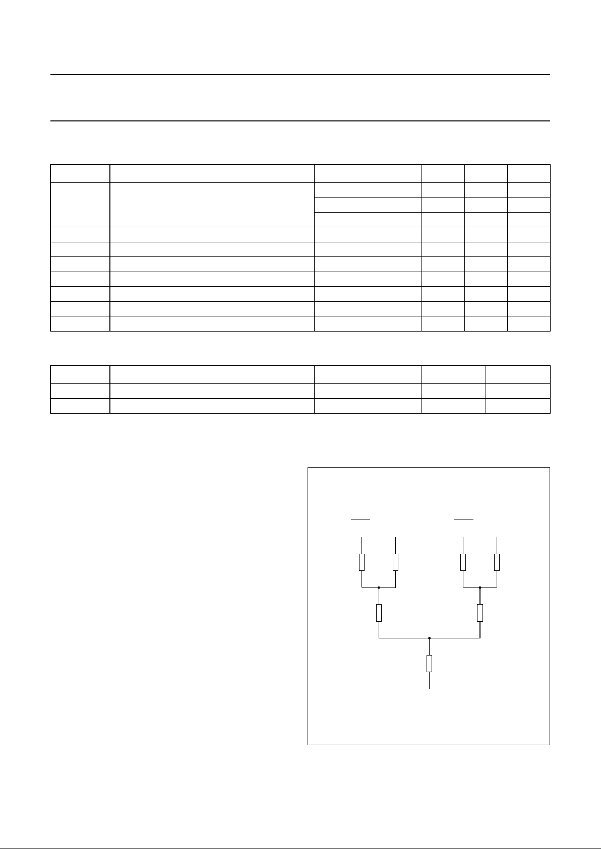
Fig.3 Thermal equivalent resistance network.

2000 Feb 09 7
Philips Semiconductors Product specification
2 × 25 W high efficiency car radio power
amplifier
TDA1563Q
DC CHARACTERISTICS
VP= 14.4 V; T
amb
=25°C; measured in Fig.7; unless otherwise specified.
Notes
1. The circuit is DC biased at V
P
= 6 to 18 V and AC operating at VP=8to18V.
2. If the junction temperature exceeds 150 °C, the output power is limited to 5 W per channel.
SYMBOL PARAMETER CONDITIONS MIN. TYP. MAX. UNIT
Supplies
V
P
supply voltage note 1 6 14.4 18 V
I
q(tot)
total quiescent current RL= ∞−95 150 mA
I
stb
standby current − 150µA
V
C
average electrolytic capacitor voltage at pin 4 − 7.1 − V
∆V
O
DC output offset voltage on state −−100 mV
mute state −−100 mV
Mode select switch (see Fig.4)
V
ms
voltage at mode select pin (pin 6) standby condition 0 − 1V
mute condition 2 − 3V
operating condition 4 5 V
P
V
I
ms
switch current through pin 6 Vms=5V − 25 40 µA
Diagnostic
V
diag
output voltage at diagnostic outputs (pins 14 and
15): protection/temperature and detection
during any fault condition −−0.5 V
I
diag
current through pin 14 or 15 during any fault condition 2 −−mA
V
SC
input voltage at selectable clip pin (pin 12) clip detect at THD = 10% −−0.5 V
clip detect at THD = 2.5% 1.5 − 18 V
Protection
T
pre
prewarning temperature − 145 −°C
T
dis(BTL)
BTL disable temperature note 2 − 150 −°C

2000 Feb 09 8
Philips Semiconductors Product specification
2 × 25 W high efficiency car radio power
amplifier
TDA1563Q
Fig.4 Switching levels of the mode select switch.
handbook, halfpage
MGR176
18
V
mode
4
3
2
1
0
Mute
Operating
Standby

2000 Feb 09 9
Philips Semiconductors Product specification
2 × 25 W high efficiency car radio power
amplifier
TDA1563Q
AC CHARACTERISTICS
VP= 14.4 V; RL=4Ω; CSE = 1000 µF; f = 1 kHz; T
amb
=25°C; measured in Fig.7; unless otherwise specified.
Notes
1. The distortion is measured with a bandwidth of 10 Hz to 30 kHz.
2. Frequency response externally fixed (input capacitors determine low frequency roll-off).
3. The SE to BTL switch voltage level depends on V
P
.
4. Noise output voltage measured with a bandwidth of 20 Hz to 20 kHz.
5. Noise output voltage is independent of Rs.
SYMBOL PARAMETER CONDITIONS MIN. TYP. MAX. UNIT
P
o
output power THD = 0.5% 15 19 − W
THD = 10% 23 25 − W
EIAJ − 38 − W
V
P
= 13.2 V; THD = 0.5% − 16 − W
V
P
= 13.2 V; THD = 10% − 20 − W
THD total harmonic distortion P
o
= 1 W; note 1 − 0.1 − %
P
d
dissipated power see Figs 10 and 11 W
B
p
power bandwidth THD= 1%; Po= −1dB
with respect to 15 W
− 20 to 15000 − Hz
f
ro(l)
low frequency roll-off −1 dB; note 2 − 25 − Hz
f
ro(h)
high frequency roll-off −1dB 130 −−kHz
G
v
closed loop voltage gain Po= 1 W 25 26 27 dB
SVRR supply voltage ripple rejection R
s
=0Ω; V
ripple
= 2 V (p-p)
on/mute 45 65 − dB
standby; f = 100 Hz to 10 kHz 80 −−dB
CMRR common mode rejection ratio R
s
=0Ω−80 − dB
Z
i
input impedance 90 120 150 kΩ
∆Z
i
mismatch in input impedance − 1 − %
V
SE-BTL
SE to BTL switch voltage level note 3 − 3 − V
V
o(mute)
output voltage mute (RMS value) Vi= 1 V (RMS) − 100 150 µV
V
n(o)
noise output voltage on; Rs=0Ω; note 4 − 100 150 µV
on; R
s
=10kΩ; note 4 − 105 −µV
mute; note 5 − 100 150 µV
α
cs
channel separation Rs=0Ω; Po=15W 40 70 − dB
∆G
v
channel unbalance −− 1dB

2000 Feb 09 10
Philips Semiconductors Product specification
2 × 25 W high efficiency car radio power
amplifier
TDA1563Q
Fig.5 Clip detection waveforms.
handbook, halfpage
MGR177
V
o
CLIP
0
0
t
Fig.5 Clip detection waveforms. Fig.6 Protection waveforms.
handbook, halfpage
MGR178
maximum current short circuit to supply pins
short circuit
to ground
short circuit
removed
50
ms
50
ms
50
ms
10 µs
I
o
DIAG
0
max
max
t
t
 Loading...