

Philips TDA1562Q-N1, TDA1562Q-N2-S10, TDA1562Q-N1-S10, TDA1562Q-N2 Datasheet

DATA SH EET
Preliminary specification
File under Integrated Circuits, IC01
1998 Apr 07
INTEGRATED CIRCUITS
TDA1562Q
70 W high efficiency power
amplifier with diagnostic facility

1998 Apr 07 2
Philips Semiconductors Preliminary specification
70 W high efficiency power amplifier
with diagnostic facility
TDA1562Q
FEATURES
• Very high output power, operating from a single low
supply voltage
• Low power dissipation, when used for music signals
• Switches to low output power at too high case
temperatures
• Few external components
• Fixed gain
• Differential inputs with high common mode rejection
• Mode select pin (on, mute and standby)
• Status I/O pin (class-H, class-B and fast mute)
• All switching levels with hysteresis
• Diagnostic pin with information about:
– Dynamic Distortion Detector (DDD)
– Any short-circuit at outputs
– Open load detector
– Temperature protection.
• No switch-on or switch-off plops
• Fast mute on supply voltage drops
• Quick start option (e.g. car-telephony/navigation)
• Low (delta) offset voltage at the outputs
• Load dump protection
• Short-circuit safe to ground, supply voltage and across
the load
• Low power dissipation in any short-circuit condition
• Protected against electrostatic discharge
• Thermally protected
• Flexible leads.
GENERAL DESCRIPTION
The TDA1562Q is a monolithic integrated 70 W/4 Ω
Bridge-Tied Load (BTL) class-H high efficiency power
amplifier in a 17-lead DIL-bent-SIL plastic power
package.
The device can be used for car audio systems (e.g. car,
radio and boosters) as well as mains fed applications (e.g.
midi/mini audio combinations and TV sound).
QUICK REFERENCE DATA
Test conditions: V
P
= 14.4 V; RL=4Ω; Rs=0Ω; f = 1 kHz; T
amb
=25°C; unless otherwise specified.
SYMBOL PARAMETER CONDITIONS MIN. TYP. MAX. UNIT
V
P
supply voltage operating 8 14.4 18 V
non-operating −−30 V
load dump −−45 V
I
q(tot)
total quiescent current on and mute;
RL= open circuit
− 110 150 mA
I
stb
standby current standby − 150µA
V
OO
output offset voltage on and mute −−100 mV
∆V
OO
delta output offset voltage on ↔ mute −−30 mV
G
v
voltage gain 25 26 27 dB
Z
i(dif)
differential input impedance 90 150 − kΩ
P
o
output power THD = 0.5% 45 55 − W
THD = 10% 60 70 − W
THD total harmonic distortion P
o
=1W − 0.03 − %
P
o
=20W − 0.06 − %
DDD active − 10 − %
SVRR supply voltage ripple rejection on and mute 60 70 − dB
CMRR common mode rejection ratio on 70 80 − dB
ISRR input signal rejection ratio mute 80 90 − dB
V
n(o)
noise output voltage on − 100 150 µV

1998 Apr 07 3
Philips Semiconductors Preliminary specification
70 W high efficiency power amplifier
with diagnostic facility
TDA1562Q
ORDERING INFORMATION
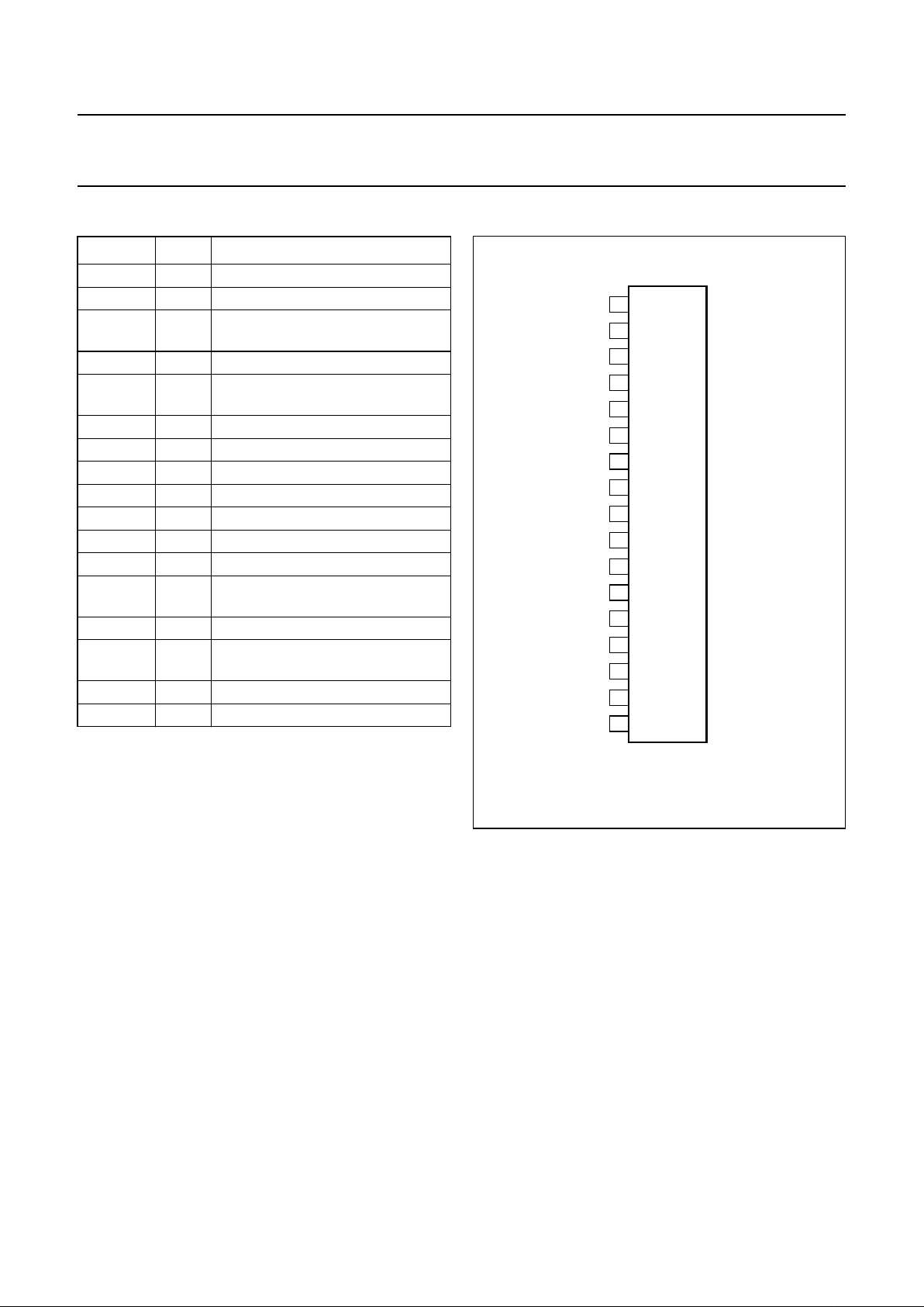
BLOCK DIAGRAM
TYPE NUMBER
PACKAGE
NAME DESCRIPTION VERSION
TDA1562Q DBS17P plastic DIL-bent-SIL power package; 17 leads (lead length 12 mm) SOT243-1
Fig.1 Block diagram.
handbook, full pagewidth
POWERSTAGE
PREAMP
status I/O
VP*
VP*
75
kΩ
−
+
C1+C1−
FEEDBACK
CIRCUIT
TDA1562Q
POWERSTAGE
CLASS-B
CLASS-H
FAST MUTE
TEMPERATURE
SENSOR
LOAD DUMP
PROTECTION
STANDBY
MUTE
ON
LOAD
DETECTOR
DYNAMIC
DISTORTION
DETECTOR
DIAGNOSTIC
INTERFACE
TEMPERATURE
PROTECTION
CURRENT
PROTECTION
LIFT-SUPPLY
LIFT-SUPPLY
disable
disable
16
mode
select
4
1
IN+
35
75
kΩ
15 kΩ
reference
voltage
PREAMP
−
+
2
IN−
14
V
ref
17
signal
GND
C2+C2−
OUT−
15 13 6
PGND1 PGND2
MGL264
12
11
diagnostic
OUT+
7
8
910
V
P2
V
P1
1998 Apr 07 4
Philips Semiconductors Preliminary specification
70 W high efficiency power amplifier
with diagnostic facility
TDA1562Q
PINNING
SYMBOL PIN DESCRIPTION
IN+ 1 signal input (positive)
IN− 2 signal input (negative)
C1− 3 negative terminal of lift electrolytic
capacitor 1
MODE 4 mode select input
C1+ 5 positive terminal of lift electrolytic
capacitor 1
PGND1 6 power ground 1
OUT+ 7 positive output
DIAG 8 diagnostic output (open collector)
V
P1
9 supply voltage 1
V
P2
10 supply voltage 2
OUT− 11 negative output
PGND2 12 power ground 2
C2+ 13 positive terminal of lift electrolytic
capacitor 2
V
ref
14 internal reference voltage
C2− 15 negative terminal of lift electrolytic
capacitor 2
STAT 16 status I/O
SGND 17 signal ground
Fig.2 Pin configuration.
handbook, halfpage
TDA1562Q
MGL263
1
2
3
4
5
6
7
8
9
10
11
12
13
14
15
16
17
IN+
IN−
C1−
MODE
C1+
PGND1
OUT+
DIAG
V
P1
V
P2
OUT−
PGND2
C2+
V
ref
C2−
STAT
SGND

1998 Apr 07 5
Philips Semiconductors Preliminary specification
70 W high efficiency power amplifier
with diagnostic facility
TDA1562Q
FUNCTIONAL DESCRIPTION
The TDA1562Q contains a mono class-H BTL output
power amplifier. At low output power, up to 18 W, the
device operates as a normal BTL amplifier. When a larger
output voltage swing is required, the internal supply
voltage is lifted by means of the external electrolytic
capacitors. Due to this momentarily higher supply voltage
the obtainable output power is 70 W.
In normal use, when the output is driven with music-like
signals, the high output power is only needed during a
small percentage of time. Under the assumption that a
music signal has a normal (Gaussian) amplitude
distribution, the reduction in dissipation is about 50% when
compared to a class-B output amplifier with the same
output power. The heatsink should be designed for use
with music signals. If the case temperature exceeds
120 °C, the device will switch back from class-H to class-B
operation. The high power supply voltage is then disabled
and the output power is limited to 20 W.
When the supply voltage drops below the minimum
operating level, the amplifier will be muted immediately.
Mode select input (pin MODE)
This pin has 3 modes:
1. LOW, ‘standby’: the complete circuit is switched off,
the supply current is very low
2. MID, ‘mute’: the circuit is switched on, but the input
signal is suppressed
3. HIGH, ‘on’: normal operation, the input signal is
amplified by 26 dB.
When the circuit is switched from mute to on or vice versa
the actual switching takes place at a zero crossing of the
input signal. The circuit contains a quick start option, i.e.
when it is switched directly from standby to on,
the amplifier is fully operational within 50 ms (important for
applications like car telephony and car navigation).
Status I/O input (pin STAT)
I
NPUT
This input has 3 possibilities:
1. LOW, ‘fast mute’: the circuit remains switched on, but
the input signal is suppressed
2. MID, ‘class-B’: the circuit operates as class-B
amplifier, the high power supply voltage is disabled,
independent of the case temperature
3. HIGH, ‘class-H’: the circuit operates as class-H
amplifier, the high power supply voltage is enabled,
independent of the case temperature.
When the circuit is switched from fast mute to class-B/H or
vice versa the switching is immediately carried out. When
the circuit is switched from class-B to class-H or vice versa
the actual switching takes place at a zero crossing of the
input signal.
O
UTPUT
This output has 3 possibilities:
1. LOW, ‘mute’: acknowledge of muted amplifier
2. MID, ‘class-B’: the circuit operates as class-B
amplifier, the high power supply voltage is disabled,
caused by the case temperature Tc> 120 °C
3. HIGH, ‘class-H’: the circuit operates as class-H
amplifier, the high power supply voltage is enabled,
because the case temperature Tc< 120 °C.
When the circuit is switched from class-B to class-H or vice
versa the actual switching takes place at a zero crossing
of the input signal.
The status I/O pins of maximum 8 devices may be tied
together for synchronizing purposes.
1998 Apr 07 6
Philips Semiconductors Preliminary specification
70 W high efficiency power amplifier
with diagnostic facility
TDA1562Q
Fig.3 Switching characteristics.
handbook, full pagewidth
on
mute
0
supply
voltage
reference
voltage
mode select
input
status I/O
input
HIGH
MID
LOW
HIGH
MID
class-H (Tc < 120 °C)
class-B (Tc > 120 °C)
LOW
status I/O
output
HIGH
MID
LOW
V
ref
VRT
0
output voltage
across load
0
zerocross change
class B/H-operation
zerocross mute
function
fast mute
function
quick start
mute
supply mute
function
MGL272
 Loading...