

Philips TDA1561Q-N2, TDA1561Q-N1 Datasheet

DATA SH EET
Preliminary specification
Supersedes data of 1997 Jun 11
File under Integrated Circuits, IC01
1997 Aug 14
INTEGRATED CIRCUITS
TDA1561Q
2 × 23 W high efficiency car radio
power amplifier
1997 Aug 14 2
Philips Semiconductors Preliminary specification
2 × 23 W high efficiency car radio power
amplifier
TDA1561Q
FEA TURES
• Low dissipation due to switching from Single-Ended
(SE) to Bridge-Tied Load (BTL) mode
• High Common Mode Rejection Ratio (CMRR)
• Mute/standby/operating/SE-only (mode select pin)
• Zero crossing mute and standby circuit
• Load dump protection circuit
• Short-circuit safe to ground, to supply voltage and
across load
• Loudspeaker protection circuit
• Device switches to single-ended operation at excessive
junction temperatures.
GENERAL DESCRIPTION
The TDA1561Q is a monolithic power amplifier in a 13 lead
single-in-line (SIL) plastic power package. It contains two
identical 23 W amplifiers. The dissipation is minimized by
switching from SE to BTL mode, only when a higher output
voltage swing is needed. The device is primarily
developed for car radio applications.
QUICK REFERENCE DATA
ORDERING INFORMATION
SYMBOL PARAMETER CONDITIONS MIN. TYP. MAX. UNIT
V
P
supply voltage DC biased 6.0 14.4 18 V
non operating −−30 V
load dump −−50 V
I
ORM
repetitive peak output current −−4A
I
q(tot)
total quiescent current RL= ∞−95 150 mA
I
stb
standby current − 150µA
Z
i
input impedance − 60 − kΩ
P
o
output power RL = 4 Ω; EIAJ − 36 − W
THD 10% 21 23 − W
G
v
voltage gain 31 32 33 dB
CMRR common mode rejection ratio f = 1 kHz; R
s
=0Ω−80 − dB
SVRR supply voltage ripple rejection f = 1 kHz; R
s
=0Ω 45 55 − dB
∆V
O
DC output offset voltage −−150 mV
α
cs
channel separation Rs=0kΩ 40 60 − dB
∆G
v
channel unbalance −−1dB
TYPE
NUMBER
PACKAGE
NAME DESCRIPTION VERSION
TDA1561Q DBS13P plastic DIL-bent-SIL power package; 13 leads (lead length 12 mm) SOT141-6
1997 Aug 14 3
Philips Semiconductors Preliminary specification
2 × 23 W high efficiency car radio power
amplifier
TDA1561Q
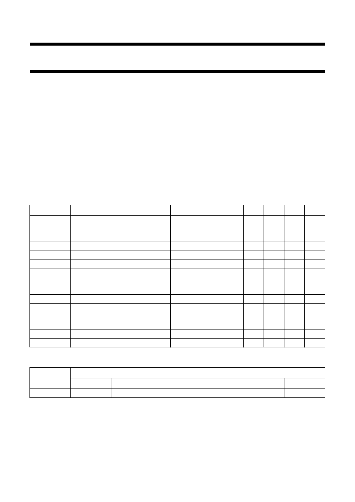
BLOCK DIAGRAM
Fig.1 Block diagram.
handbook, full pagewidth
MLD214
REFERENCE
SOURCES
MUTE/STANDBY
THERMAL/
SHORT-CIRCUIT
PROTECTION
HIGHER
TEMPERATURE
BTL DISABLE
0.5V
P
MUTE
R
MUTE
R
7
V
P
12
3
13
2
1
IN1
IN2
CIN
MODE
1/2R
HV
4
GND1
10
GND2
6
5
11
9
8
OUT2
OUT2
OUT1
OUT1
C
TDA1561Q
P
11
1997 Aug 14 4
Philips Semiconductors Preliminary specification
2 × 23 W high efficiency car radio power
amplifier
TDA1561Q
PINNING
SYMBOL PIN DESCRIPTION
IN1 1 input 1
HV
P
2 half supply voltage control input
MODE 3 mute/standby/operating/SE-only
GND1 4 ground 1
OUT1 5 inverting output 1
OUT1 6 non-inverting output 1
V
P
7 supply voltage
OUT2 8 inverting output 2
OUT2 9 non-inverting output 2
GND2 10 ground 2
C
11
11 electrolytic capacitor for
single-ended (SE) mode
CIN 12 common input
IN2 13 input 2
Fig.2 Pin configuration.
handbook, halfpage
MLD215
1
2
3
4
5
6
7
8
9
10
11
12
13
TDA1561Q
IN1
HV
GND1
OUT1
V
MODE
OUT1
OUT2
11
C
CIN
IN2
GND2
OUT2
P
P

1997 Aug 14 5
Philips Semiconductors Preliminary specification
2 × 23 W high efficiency car radio power
amplifier
TDA1561Q
FUNCTIONAL DESCRIPTION
The TDA1561Q contains two identical amplifiers with
differential inputs. At low output power (up to output
amplitudes of 3 V (RMS) at VP= 14.4 V), the device
operates as a normal SE amplifier. When a larger output
voltage swing is needed, the circuit switches internally to
BTL operation.
With a sine wave input signal the dissipation of a
conventional BTL amplifier up to 2 W output power is more
than twice the dissipation of the TDA1561Q (see Fig.9).
In normal use, when the amplifier is driven with music-like
signals, the high (BTL) output power is only needed for a
small percentage of time. Under the assumption that a
music signal has a normal (Gaussian) amplitude
distribution, the dissipation of a conventional BTL amplifier
with the same output power is approximately 70% higher
(see Fig.10).
The heatsink has to be designed for use with music
signals. With such a heatsink, the thermal protection will
disable the BTL mode when the junction temperature
exceeds 145 °C. In this case the output power is limited to
5 W per amplifier.
The gain of each amplifier is internally fixed at 32 dB. With
the MODE pin, the device can be switched to the following
modes:
• Standby with low standby current (<50 µA)
• Mute condition, DC adjusted
• On, operation
• SE-only, operation (BTL disabled).
The device is fully protected against short-circuiting of the
output pins to ground and to the supply voltage. It is also
protected against short-circuiting the loudspeaker and
high junction temperatures. In the event of a permanent
short-circuit condition to ground or the supply voltage, the
output stage will be switched off causing a low dissipation.
With permanent short-circuiting of the loudspeaker, the
output stage will be repeatedly switched on and off.
The duty cycle in the ‘on’ condition is low enough to
prevent excessive dissipation.
To avoid plops during switching from ‘mute’ to ‘on’ or from
‘on’ to ‘mute/standby’ while an input signal is present, a
built-in zero-crossing detector allows only switching at
zero input voltage. However, when the supply voltage
drops below 6 V (e.g. engine start), the circuit mutes
immediately avoiding clicks coming from electronic
circuitry preceding the power amplifier.
The voltage of the SE electrolytic capacitor (pin 11) is
always kept at 0.5V
P
by means of a voltage buffer (see
Fig.1). The value of this capacitor has an important
influence on the output power in SE mode, especially at
low signal frequencies, a high value is recommended to
minimize dissipation at low frequencies.

1997 Aug 14 6
Philips Semiconductors Preliminary specification
2 × 23 W high efficiency car radio power
amplifier
TDA1561Q
LIMITING VALUES
In accordance with the Absolute Maximum Rating System (IEC 134).
THERMAL CHARACTERISTICS
Note
1. The value of R
th(c-h)
depends on the application (see Fig.3).
SYMBOL PARAMETER CONDITIONS MIN. MAX. UNIT
V
P
supply voltage operating − 18 V
non operating − 30 V
load dump; tr> 2.5 ms − 50 V
V
P(sc)
short-circuit safe voltage − 18 V
V
rp
reverse polarity voltage − 6V
I
OSM
non-repetitive peak output current − 6A
I
ORM
repetitive peak output current − 4A
P
tot
total power dissipation − 60 W
T
stg
storage temperature −55 +150 °C
T
vj
virtual junction temperature − 150 °C
T
amb
operating ambient temperature −40 −°C
SYMBOL PARAMETER CONDITIONS VALUE UNIT
R
th(j-c)
thermal resistance from junction to case see note 1 1.3 K/W
R
th(j-a)
thermal resistance from junction to ambient 40 K/W
1997 Aug 14 7
Philips Semiconductors Preliminary specification
2 × 23 W high efficiency car radio power
amplifier
TDA1561Q
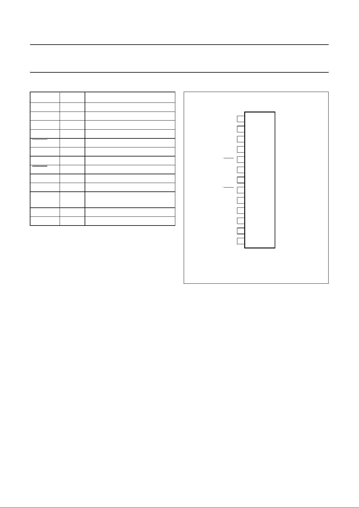
Heatsink design
There are two parameters that determine the size of the
heatsink. The first is the rating for the virtual junction
temperature and the second is the ambient temperature at
which the amplifier must still deliver its full power in the
BTL mode.
With a conventional BTL amplifier, the maximum power
dissipation with a music-like signal (at each amplifier) will
be approximately two times 5 W. At a virtual junction
temperature of 150 °C and a maximum ambient
temperature of 60 °C, R
th(vj-c)
= 1.3 K/W and
R
th(c-h)
= 0.2 K/W, the thermal resistance of the heatsink
should be:
Compared to a conventional BTL amplifier, the TDA1561Q
has a higher efficiency. The thermal resistance of the
heatsink should be:
150 60–
25×
----------------------
1.3– 0.2– 7.5 K/W=
1.7
150 60–
25×
----------------------
1.3– 0.2– 13.8 K/W=
Fig.3 Thermal equivalent resistance network.
handbook, halfpage
3.6 K/W
0.6 K/W
3.6 K/W
virtual junction
OUT 1 OUT 1
case
3.6 K/W
0.6 K/W
3.6 K/W
OUT 2 OUT 2
MGC424
0.1 K/W
1997 Aug 14 8
Philips Semiconductors Preliminary specification
2 × 23 W high efficiency car radio power
amplifier
TDA1561Q
DC CHARACTERISTICS
V
P
= 14.4 V; T
amb
=25°C; measured in Fig.6; unless otherwise specified.
Note
1. The circuit is DC biased at V
P
= 6 to 18 V and AC operating at VP=8to18V.
SYMBOL PARAMETER CONDITIONS MIN. TYP. MAX. UNIT
Supplies
V
P
supply voltage note 1 6.0 14.4 18.0 V
I
q
quiescent current RL= ∞−95 150 mA
I
stb
standby current − 150µA
V
C
average electrolytic capacitor
voltage at pin 11
− 7.1 − V
∆V
O
DC output offset voltage on state −−150 mV
mute state −−50 mV
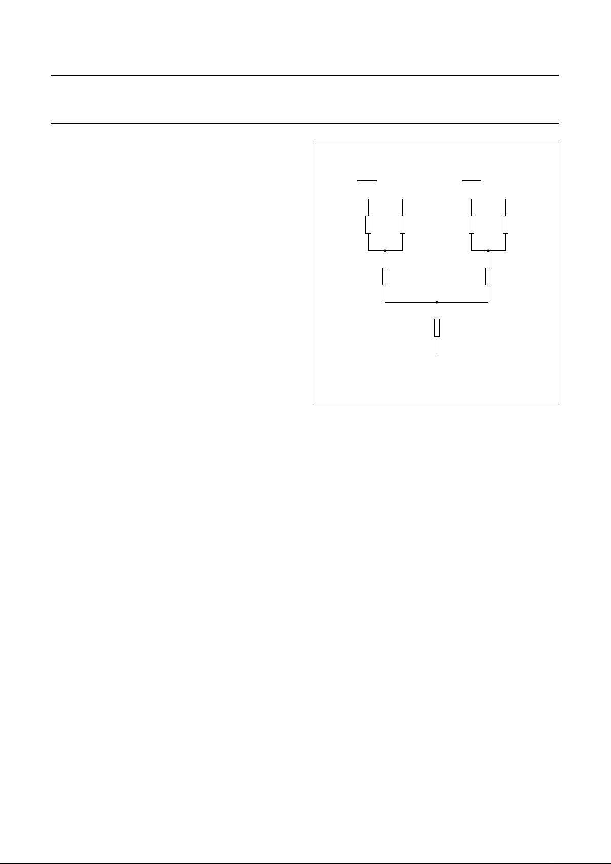
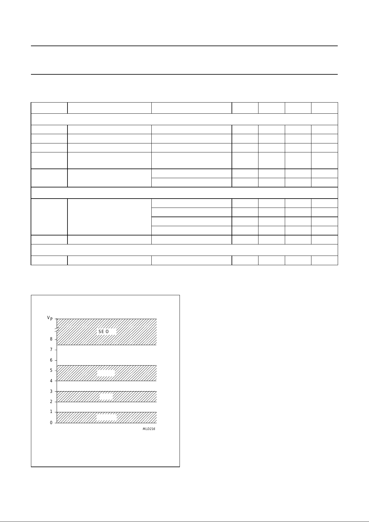
Mode select switch (see Fig.4)
V
ms
voltage at mode select pin
(pin 3)
standby condition 0 − 1V
mute condition 2 − 3V
on condition (SE/BTL mode) 4 − 5.5 V
on condition (SE mode only) 7.5 − V
P
V
I
ms
switch current through pin 3 Vms=5V −−40 µA
Protection
T
dis
BTL disable temperature − 145 −°C
Fig.4 Switching levels of mode select switch.
handbook, halfpage
,,,,,
,
0
MLD216
V
1
2
3
4
5
6
7
8
P
SE Only
SE/BTL
Standby
Mute
 Loading...