

Philips TDA1555Q Datasheet

INTEGRATED CIRCUITS
DATA SH EET
TDA1555Q
4 x 11 W single-ended or 2 x 22 W
power amplifier with distortion
detector
Product specification
File under Integrated Circuits, IC01
May 1992

Philips Semiconductors Product specification
4 x 1 1 W single-ended or 2 x 22 W power
TDA1555Q
amplifier with distortion detector
GENERAL DESCRIPTION
The TDA1555Q is an integrated class-B output amplifier in a 17-lead single-in-line (SIL) plastic power package.
The circuit contains 4 x 11 W single-ended or 2 x 22 W bridge amplifiers. The device is primarily developed for car radio
applications.
Features
• Requires very few external components
• Flexibility in use − Quad single-ended or stereo BTL
• High output power
• Low offset voltage at outputs (important for BTL)
• Fixed gain
• Good ripple rejection
• Mute/stand-by switch
• Load dump protection
• AC and DC short-circuit-safe to ground and V
P
QUICK REFERENCE DATA
• Thermally protected
• Reverse polarity safe
• Capability to handle high energy on outputs (VP = 0 V)
• Protected against electrostatic discharge
• No switch-on/switch-off plop
• Low thermal resistance
• Identical inputs (inverting and non-inverting)
• Flexible leads
• Distortion detector.
PARAMETER CONDITIONS SYMBOL MIN. TYP. MAX. UNIT
Supply voltage range
operating V
Repetitive peak output current I
Total quiescent current I
Stand-by current I
P
ORM
tot
sb
6.0 14.4 18.0 V
−−4A
− 80 160 mA
− 0.1 100 µA
Stereo BTL application
Output power RL = 4 Ω; THD = 10% P
o
20 22 − W
Supply voltage ripple rejection RR 48 −−dB
Noise output voltage
(RMS value) R
= 0 Ω V
S
no(rms)
Input impedance |Z
DC output offset voltage |∆V
| 253038kΩ
I
O
− 70 −µV
| −−100 mV
Quad single-ended application
Output power THD = 10%
R
= 4 Ω P
L
= 2 Ω P
R
L
o
o
− 6 − W
− 11 − W
Supply voltage ripple rejection RR 48 −−dB
Noise output voltage
(RMS value) R
= 0 Ω V
S
Input impedance |Z
no(rms)
| 506075kΩ
I
− 50 −µV
PACKAGE OUTLINE
17-lead SIL-bent-to-DIL; plastic power (SOT243R); SOT243-1; 1996 July 23.
May 1992 2
Philips Semiconductors Product specification
4 x 11 W single-ended or 2 x 22 W power
amplifier with distortion detector
TDA1555Q
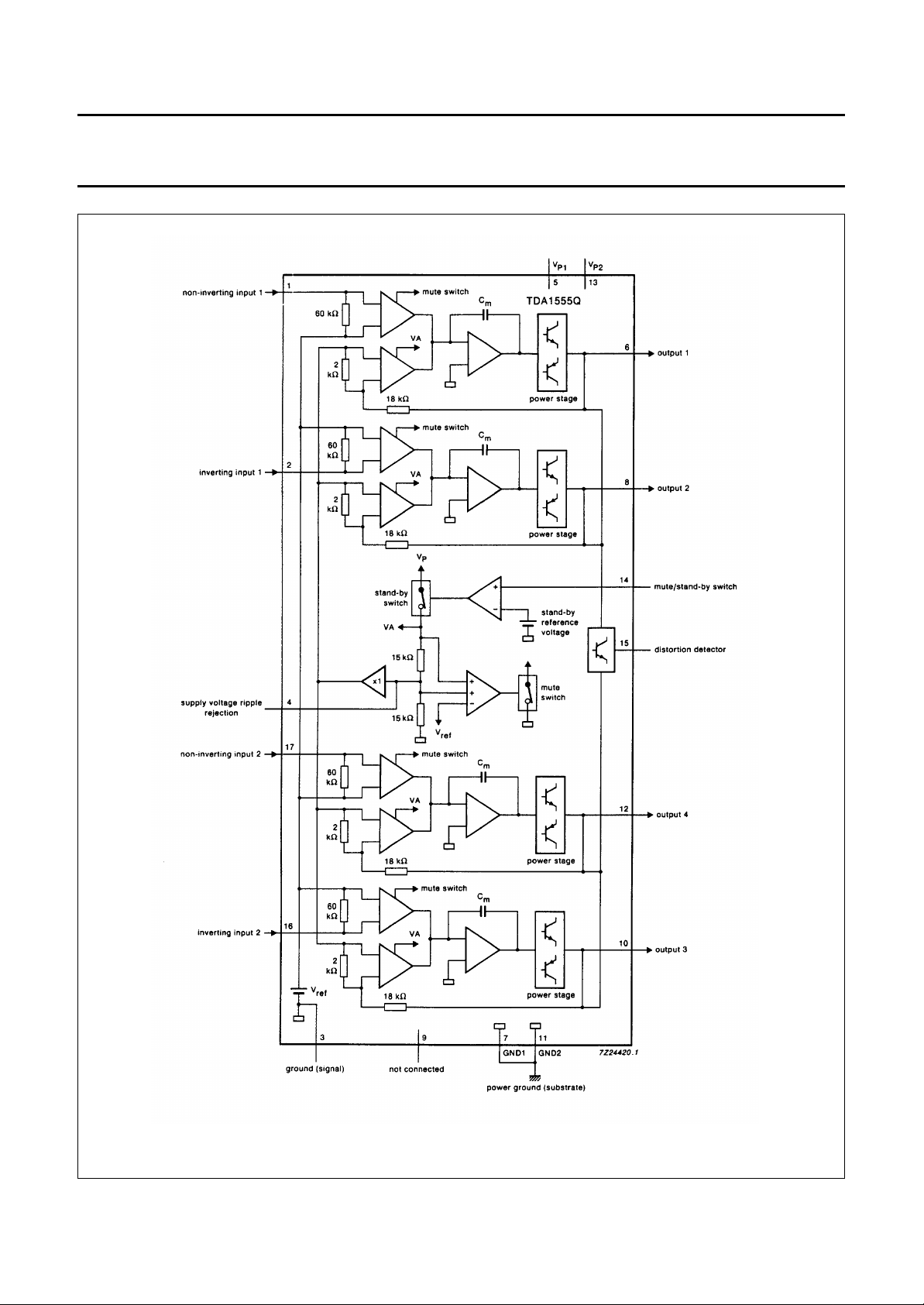
Fig.1 Block diagram.
May 1992 3

Philips Semiconductors Product specification
4 x 11 W single-ended or 2 x 22 W power
TDA1555Q
amplifier with distortion detector
PINNING
1 NINV1 non-inverting input 1 9 n.c. not connected
2 INV1 inverting input 1 10 OUT3 output 3
3 GND ground (signal) 11 GND2 power ground 2 (substrate)
4 RR supply voltage ripple rejection 12 OUT4 output 4
5V
P1
positive supply voltage 1 13 V
P2
6 OUT1 output 1 14 M/SS mute/stand-by switch
7 GND1 power ground 1 (substrate) 15 DD distortion detector
8 OUT2 output 2 16 INV2 inverting input 2
17 NINV2 non-inverting input 2
FUNCTIONAL DESCRIPTION
The TDA1555Q contains four identical amplifiers with differential input stages (two inverting and two non-inverting) and
can be used for single-ended or bridge applications. The gain of each amplifier is fixed at 20 dB (26 dB in BTL). Special
features of this device are:
Mute/stand-by switch
positive supply voltage 2
• low stand-by current (< 100 µA)
• low mute/stand-by switching current (low cost supply switch)
• mute facility
Distortion detector
• At onset of clipping of one or more channels the distortion detector (pin 15) becomes active. This information can be
used to drive a sound processor or DC volume control to decrease the input signal and so limit distortion.
RATINGS
Limiting values in accordance with the Absolute Maximum System (IEC 134)
PARAMETER CONDITIONS SYMBOL MIN. MAX. UNIT
Supply voltage
operating V
non-operating V
P
P
− 18 V
− 30 V
load dump protected during 50 ms;
≥ 2.5 ms V
t
r
Non-repetitive peak output current I
Repetitive peak output current I
Storage temperature range T
Junction temperature T
AC and DC short-circuit-safe voltage V
Energy handling capability at outputs V
= 0 V − 200 mJ
P
Reverse polarity V
Total power dissipation see Fig.2 P
P
OSM
ORM
stg
j
PSC
PR
tot
− 45 V
− 6A
− 4A
−55 + 150 °C
− 150 °C
− 18 V
− 6V
− 60 W
May 1992 4
 Loading...