

Philips TDA1554Q Datasheet

INTEGRATED CIRCUITS
DATA SH EET
TDA1554Q
4 x 11 W single-ended or 2 x 22 W
power amplifier
Product specification
File under Integrated Circuits, IC01
May 1992

Philips Semiconductors Product specification
4 x 1 1 W single-ended or 2 x 22 W power
TDA1554Q
amplifier
GENERAL DESCRIPTION
The TDA1554Q is an integrated class-B output amplifier in a 17-lead single-in-line (SIL) plastic power package.
The circuit contains 4 x 11 W single-ended or 2 x 22 W bridge amplifiers. The device is primarily developed for car radio
applications.
Features
• Requires very few external components
• Flexibility in use − Quad single-ended or stereo BTL
• High output power
• Low offset voltage at outputs (important for BTL)
• Fixed gain
• Good ripple rejection
• Mute/stand-by switch
• Load dump protection
• AC and DC short-circuit-safe to ground and V
P
QUICK REFERENCE DATA
• Thermally protected
• Reverse polarity safe
• Capability to handle high energy on outputs (VP = 0 V)
• Protected against electrostatic discharge
• No switch-on/switch-off plop
• Low thermal resistance
• Identical inputs (inverting and non-inverting)
• Flexible leads.
PARAMETER CONDITIONS SYMBOL MIN. TYP. MAX. UNIT
Supply voltage range
operating V
Repetitive peak output current I
Total quiescent current I
Stand-by current I
P
ORM
tot
sb
6.0 14.4 18.0 V
−−4A
− 80 160 mA
− 0.1 100 µA
Stereo BTL application
Output power R
= 4 Ω; THD = 10% P
L
o
20 22 − W
Supply voltage ripple rejection RR 48 −−dB
Noise output voltage
(RMS value) R
Input impedance |Z
DC output offset voltage |∆V
= 0 Ω V
S
no(rms)
| 253038kΩ
I
| −−100 mV
o
− 70 −µV
Quad single-ended application
Output power THD = 10%
R
= 4 Ω P
L
R
= 2 Ω P
L
o
o
− 6 − W
− 11 − W
Supply voltage ripple rejection RR 48 −−dB
Noise output voltage
(RMS value) R
Input impedance |Z
= 0 Ω V
S
no(rms)
| 506075kΩ
I
− 50 −µV
PACKAGE OUTLINE
17-lead SIL-bent-to-DIL; plastic power (SOT243R); SOT243-1; 1996 July 23.
May 1992 2
Philips Semiconductors Product specification
4 x 11 W single-ended or 2 x 22 W power
amplifier
TDA1554Q
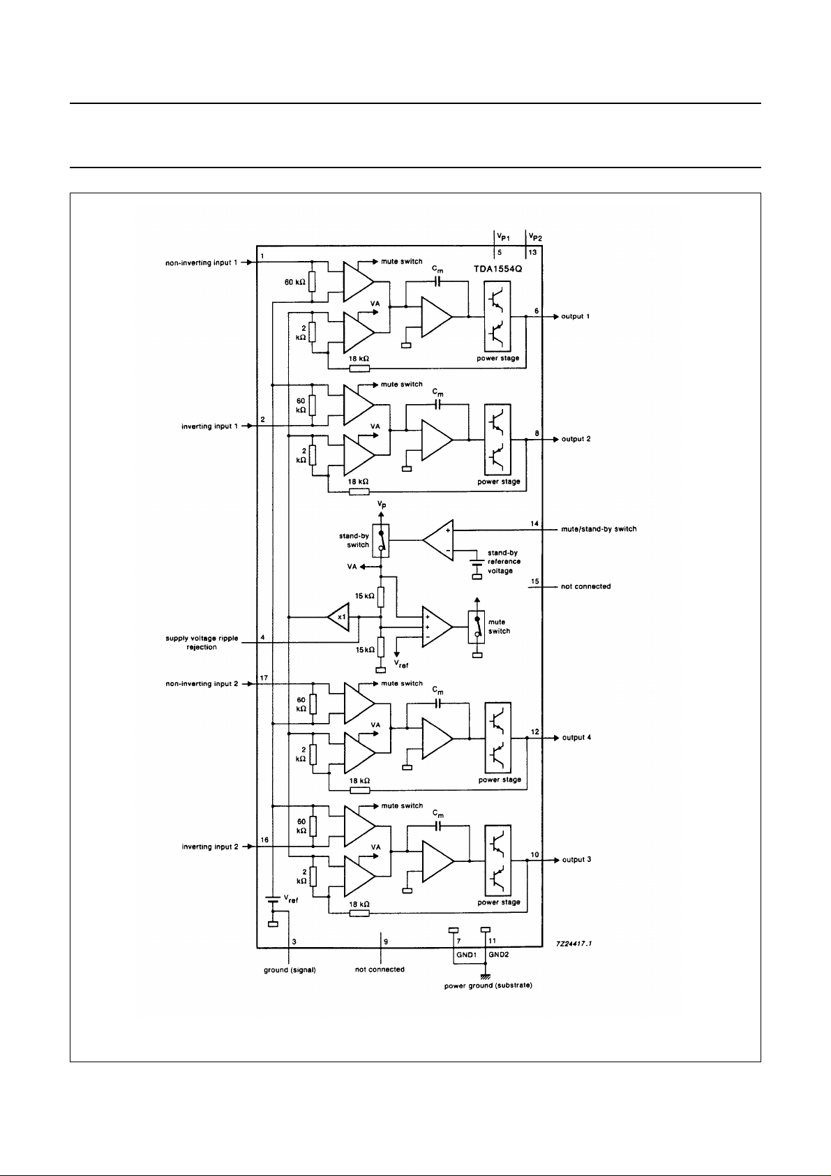
Fig.1 Block diagram.
May 1992 3

Philips Semiconductors Product specification
4 x 11 W single-ended or 2 x 22 W power
TDA1554Q
amplifier
PINNING
1 NINV1 non-inverting input 1 9 n.c. not connected
2 INV1 inverting input 1 10 OUT3 output 3
3 GND ground (signal) 11 GND2 power ground 2 (substrate)
4 RR supply voltage ripple rejection 12 OUT4 output 4
5V
P1
positive supply voltage 1 13 V
P2
6 OUT1 output 1 14 M/SS mute/stand-by switch
7 GND1 power ground 1 (substrate) 15 n.c. not connected
8 OUT2 output 2 16 INV2 inverting input 2
17 NINV2 non-inverting input 2
FUNCTIONAL DESCRIPTION
The TDA1554Q contains four identical amplifiers with differential input stages (two inverting and two non-inverting) and
can be used for single-ended or bridge applications. The gain of each amplifier is fixed at 20 dB (26 dB in BTL). A special
feature of this device is:
Mute/stand-by switch
positive supply voltage 2
• low stand-by current (< 100 µA)
• low mute/stand-by switching current (low cost supply switch)
• mute facility
RATINGS
Limiting values in accordance with the Absolute Maximum System (IEC 134)
PARAMETER CONDITIONS SYMBOL MIN. MAX. UNIT
Supply voltage
operating V
non-operating V
P
P
load dump protected during 50 ms;
t
≥ 2.5 ms V
r
Non-repetitive peak output current I
Repetitive peak output current I
Storage temperature range T
Junction temperature T
AC and DC short-circuit-safe voltage V
Energy handling capability at outputs V
= 0 V − 200 mJ
P
Reverse polarity V
Total power dissipation see Fig.2 P
P
OSM
ORM
stg
j
PSC
PR
tot
− 18 V
− 30 V
− 45 V
− 6A
− 4A
−55 + 150 °C
− 150 °C
− 18 V
− 6V
− 60 W
May 1992 4
 Loading...