

Philips TDA1551Q Datasheet

INTEGRATED CIRCUITS
DATA SH EET
TDA1551Q
2 x 22 W BTL car radio power
amplifier with diagnostic facility
Preliminary specification
File under Integrated Circuits, IC01
July 1994

Philips Semiconductors Preliminary specification
2 x 22 W BTL car radio power amplifier
with diagnostic facility
FEATURES
• Requires very few external components
• Flexible in use - quad, single ended or stereo BTL
• I2C-bus control
• Dynamic distortion detector
• Thermal protection
• Output status information
• Power supply dip detection
• High output power
• MUTE/sleep mode by writing to I2C-bus
• Stand-by mode
• Fixed gain
• Good ripple rejection
• Load dump protection
• AC/DC short circuit safe to ground and V
• Reverse polarity safe
• Low offset voltage at output
• Capable of handling high energy at outputs (VP= 0 V)
P
TDA1551Q
• Electrostatic discharge protection
• No switch-ON/switch-OFF plop
• Flexible leads
• Low thermal resistance
• Identical inputs (inverting and non-inverting).
DESCRIPTION
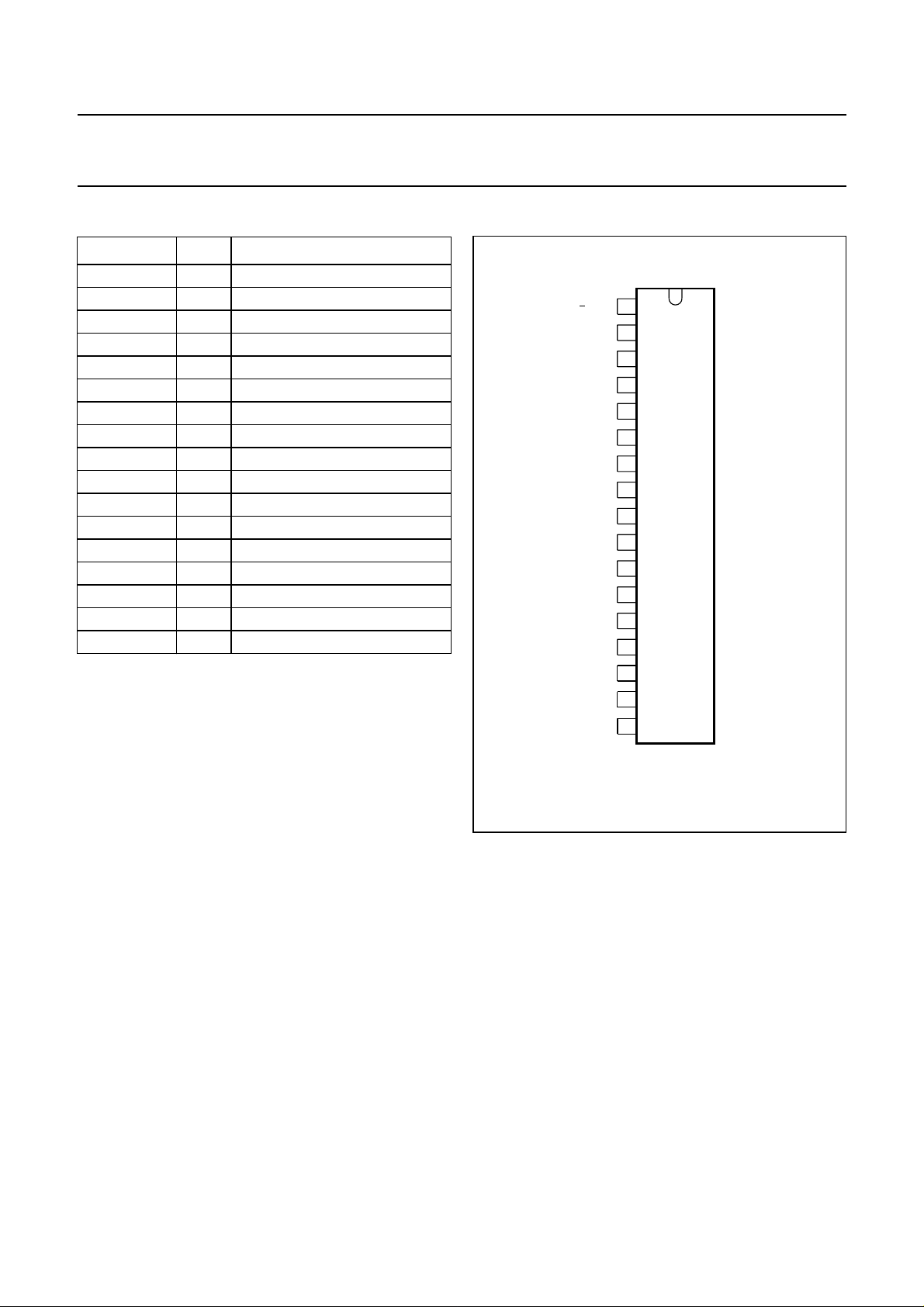
The TDA1551Q is an integrated class-B output amplifier
encased in a 17-lead single-in-line plastic power package.
The device contains 4 ×11 W single-ended (SE) or 2 × 22
W BTL amplifiers and is intended for use in car radio
applications.
QUICK REFERENCE DATA
SYMBOL PARAMETER CONDITIONS MIN. TYP. MAX. UNIT
V
P
V
P
I
P
supply voltage range operating 6 14.4 18 V
supply voltage non-operating −−30 V
total quiescent current − 80 160 mA
Quad-single-ended application
P
o
V
no
output power RL= 4 Ω; THD = 10 % − 6 − W
R
= 2 Ω; THD = 10 % − 11 − W
L
output voltage noise RS= 0 Ω−50 −µV
Stereo BTL application
P
o
V
no
∆V
o
output power RL= 4 Ω; THD = 10 % − 22 − W
output voltage noise RS= 0 Ω−70 −µV
DC output offset voltage −−100 mV
ORDERING INFORMATION
EXTENDED TYPE
NUMBER
PINS PIN POSITION MATERIAL CODE
PACKAGE
TDA1551Q 17 SIL bent to DIL plastic SOT243R
(1)
Note
1. SOT243-1; 1996 September 06.
July 1994 2

Philips Semiconductors Preliminary specification
2 x 22 W BTL car radio power amplifier
with diagnostic facility
TDA1551Q
Fig.1 Block diagram.
July 1994 3
Philips Semiconductors Preliminary specification
2 x 22 W BTL car radio power amplifier
with diagnostic facility
PINNING
SYMBOL PIN DESCRIPTION
−INV1 1 non-inverting input 1
INV1 2 inverting input 1
GND 3 signal ground
V
PRR
V
p1
OUT1 6 output 1
GND1 7 power ground 1
OUT2 8 output 2
SB 9 standby
OUT3 10 output 3
GND2 11 power ground 2
OUT4 12 output 4
V
p2
INV2 14 inverting input 2
−INV2 15 non-inverting input 2
SCL 16 serial clock line
SDA 17 serial data line
4 supply voltage ripple rejection
5 positive supply voltage 1
13 positive supply voltage 2
handbook, halfpage
INV1
INV1
SGND
V
PRR
V
P
OUT1
PGDN1
OUT2
STBY
OUT3
PGND2
OUT4
INV2
NINV2
1
2VP
1
2
3
4
5
6
7
8
TDA1551Q
9
10
11
12
13
14
15
TDA1551Q
SCL
16
SDA
17
MLA007
Fig.2 Pin configuration
July 1994 4

Philips Semiconductors Preliminary specification
2 x 22 W BTL car radio power amplifier
TDA1551Q
with diagnostic facility
FUNCTIONAL DESCRIPTION
The TDA1551Q contains four identical amplifiers with differential input stages (two inverting and two non-inverting) which
can be used in SE or BTL applications. The gain of each amplifier is fixed at 20 dB for SE and 26 dB for BTL. The device
also contains an I2C-bus facility which operates in the read or write mode.
In the write mode the device can be switched to either the sleep condition (low sleep current of 0.6 mA typ.), the MUTE
condition or the ON condition.
In the read mode an 8-bit status word is available. Data bits D0 to D3 contain status information of each of the 4 outputs.
If the device is switched to the ON or MUTE condition and there is a short-circuit at one or more outputs, the power
transistors will be outside their safe operating area consequently one or more bits of D0 to D3 will be HIGH. Bits D0 to
D3 are LOW when in the normal safe operating area. Bit D4 is normally LOW if one or more channels reaches the clipping
level D4 will go HIGH. Bit D5 is normally LOW, if the crystal temperature reaches 150 °C D5 will go HIGH. After a
power-on reset bit 7 will go HIGH and a dip in the power supply will be noticed. Bit 7 will go LOW after the I
read. When pin 9 is LOW the device will switch OFF and the supply current will be reduced to 0.1 mA (max.).
virtual junction
handbook, halfpage
6 8 10 12
2
C-bus is
4 K/W
0.8 K/W
0.1 K/W
MLA009
Fig.3 Thermal equivalent resistance network.
July 1994 5
Philips Semiconductors Preliminary specification
2 x 22 W BTL car radio power amplifier
TDA1551Q
with diagnostic facility
LIMITING VALUES
In accordance with the Absolute Maximum System (IEC134)
SYMBOL PARAMETER MIN. MAX. UNIT
Supply voltage
V
P
V
P
IOSM non-repetitive peak output current − 6A
IORM repetitive peak output current − 4A
T
stg
T
c
V
Psc
V
Pr
P
tot
operating voltage − 18 V
non-operating voltage − 30 V
load dump protect − 45 V
storage temperature range −55 150 °C
crystal temperature − 150 °C
AC/DC short-circuit safe voltage − 18 V
energy handling capability at outputs (V
= 0) − 200 mJ
P
reverse polarity − 6V
total power dissipation − 60 W
QUALITY SPECIFICATION
Electrostatic handling.
SYMBOL PINS MIN. MAX. UNIT
Human body model; R
V
es
1, 2, 14, 15, 16, and 17 −1.5 +1.5 kV
= 1500 Ω; C = 100 pF
S
other −2 +2kV
Machine model; RS= 0 Ω; C = 200 pF
V
es
1, 2, 14, 15, 16, and 17 −100 +100 V
other −200 +200 V
THERMAL RESISTANCE
SYMBOL PARAMETER THERMAL RESISTANCE
R
R
th j-c
th j-a
from junction to case (Fig.3) 1.5 K/W
from junction to ambient in free air 40 K/W
July 1994 6
 Loading...