

Philips tda1549 DATASHEETS
INTEGRATED CIRCUITS
DATA SH EET
TDA1549T
Stereo 4f
data input up-sampling
s
filter with bitstream continuous
calibration DAC (BCC-DAC1)
Objective specification
File under Integrated Circuits, IC01
Philips Semiconductors
August 1994
Philips Semiconductors Objective specification
Stereo 4fs data input up-sampling filter with
bitstream continuous calibration DAC (BCC-DAC1)
FEATURES
• Easy application
• Finite-duration impulse-response (FIR) filtering and
noise shaping incorporated
• 2nd-order noise shaper
• Wide dynamic range (true 18-bit resolution)
• Low total harmonic distortion
• No zero-crossing distortion
• Superior signal-to-noise ratio
• Bitstream continuous calibration conversion concept
• Inherently monotonic
• Voltage output (1.5 V RMS) at line drive level
• Single supply rail (3.8 to 5.5 V)
• Optimum output voltage level over the entire supply
range
• Small outline packaging (SO16)
• Wide operating temperature range (−30 to +85 °C)
• Standard Japanese input format
• No analog post-filtering required
• Low power consumption
• Integrated operational amplifiers.
filtering is required. The circuit accepts 18-bit four times
oversampled input data (4f
Internal FIR filters remove the main spectral components
and increase the sampling rate to 96 times (96fs). A 2nd
order noise shaper converts this oversampled data to a
5-bit data stream. For low signal levels the converter
operates in the 1-bit bitstream mode with attendant high
differential linearity. Higher level signals are reproduced
using the dynamic continuous calibration technique,
thereby guaranteeing high linearity independent of
process variations, temperature effects and product
ageing.
High-precision, low-noise amplifiers convert the
digital-to-analog current to an output voltage capable of
driving a line output. Externally connected capacitors
perform the required 1st order filtering so that no further
post-filtering is required.
TDA1549T
) in standard Japanese format.
s
GENERAL DESCRIPTION
The TDA1549T (BCC-DAC1) is the first of a new
generation of digital-to-analog converters featuring a
unique combination of bitstream and continuous
calibration concepts.
A system of digital filtering, high oversampling, 2nd order
noise shaping and continuous calibration digital-to-analog
conversion ensures that only simple 1st order analog
ORDERING INFORMATION
TYPE NUMBER
NAME DESCRIPTION VERSION
TDA1549T SO16 plastic small outline package; 16 leads; body width 7.5 mm SOT162−1
Internal reference circuitry ensures that the output voltage
is proportional to the supply voltage, thereby making
optimum use of the supply voltage over a wide range
(3.8 to 5.5 V). This unique configuration of bitstream and
continuous calibration techniques, together with a high
degree of analog and digital integration, results in a
digital-to-analog conversion system with true 18-bit
dynamic range, high linearity and simple low-cost
application.
PACKAGE
August 1994 2
Philips Semiconductors Objective specification
Stereo 4fs data input up-sampling filter with
TDA1549T
bitstream continuous calibration DAC (BCC-DAC1)
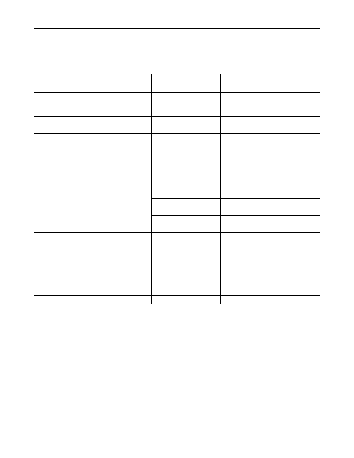
QUICK REFERENCE DATA
SYMBOL PARAMETER CONDITIONS MIN. TYP. MAX. UNIT
V
DDD
V
DDA
V
DDO
I
DDD
I
DDA
I
DDO
P
tot
V
FS(rms)
(THD + N)/S total harmonic distortion plus
S/N signal-to-noise ratio at bipolar
t
cs
BR input bit rate at data input −− 9.216 Mbits
f
BCK
TC
FS
T
amb
digital supply voltage note 1 3.8 5.0 5.5 V
analog supply voltage note 1 3.8 5.0 5.5 V
operational amplifier supply
note 1 3.8 5.0 5.5 V
voltage
digital supply current note 2 − 12 18 mA
analog supply current note2 − 5.5 8 mA
operational amplifier supply
note 2 − 6.5 9 mA
current
total power dissipation note 2 − 120 185 mW
note 3 − 50 − mW
full-scale output voltage (RMS
V
DDD=VDDA =VDDO
= 5 V 1.425 1.500 1.575 V
value)
at 0 dB signal level −−90 −83 dB
noise-to-signal ratio
− 0.003 0.007 %
at −60 dB signal level −−48 −40 dB
− 0.40 1.0 %
zero
at −60 dB signal level;
A-weighted
A-weighted;
at code 00000H
−−50 − dB
− 0.38 − %
100 110 − dB
current setting time to ±1 LSB − 0.1 −µs
input clock frequency −− 9.216 MHz
full-scale temperature
−±100 x 10
−6
−
coefficient at analog outputs
(VOL and VOR)
operating ambient temperature −30 − +85 °C
Notes
1. All V
2. Measured with V
3. Measured with V
and ground pins must be connected externally to the same supply.
DD
, V
DDD
DDD
, V
DDA
DDA
and V
and V
= 5 V at input data code 00000H.
DDO
= 3.8 V at input data code 00000H.
DDO
August 1994 3
Philips Semiconductors Objective specification
Stereo 4fs data input up-sampling filter with
bitstream continuous calibration DAC (BCC-DAC1)
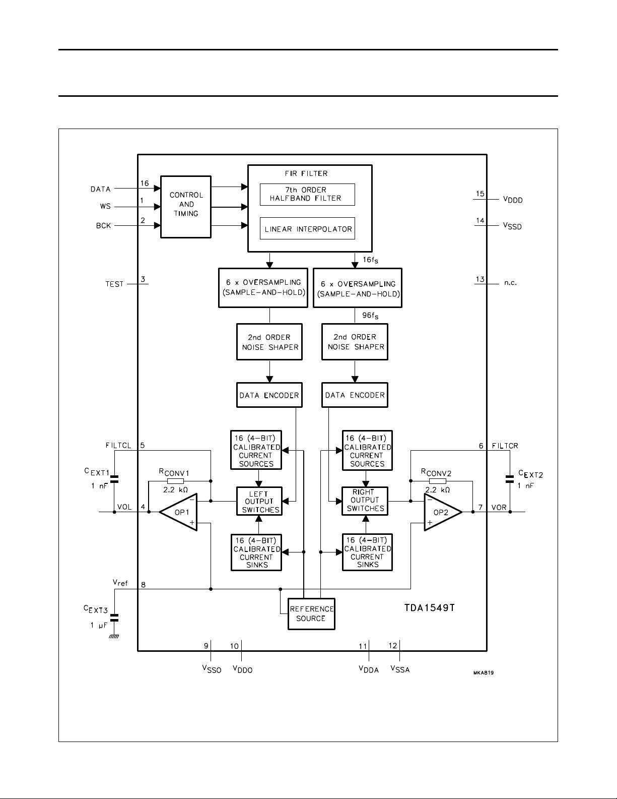
BLOCK DIAGRAM
TDA1549T
Fig.1 Block diagram.
August 1994 4

Philips Semiconductors Objective specification
Stereo 4fs data input up-sampling filter with
bitstream continuous calibration DAC (BCC-DAC1)
PINNING
SYMBOL PIN DESCRIPTION
WS 1 word select input
BCK 2 bit clock input
TEST 3 test input; pin should be connected to
ground
VOL 4 left channel output
FILTCL 5 capacitor for left channel 1st order
filter function; should be connected
between pins 4 and 5
FILTCR 6 capacitor for right channel 1st order
filter function; should be connected
between pins 6 and 7
VOR 7 right channel output
V
ref
V
SSO
V
DDO
V
DDA
V
SSA
n.c. 13 not connected (this pin should be left
V
SSD
V
DDD
DATA 16 data input
8 internal reference voltage for output
channels (1⁄2VDD)
9 operational amplifier ground
10 operational amplifier supply voltage
11 analog supply voltage
12 analog ground
open-circuit)
14 digital ground
15 digital supply voltage
TDA1549T
Fig.2 Pin configuration.
August 1994 5

Philips Semiconductors Objective specification
Stereo 4fs data input up-sampling filter with
bitstream continuous calibration DAC (BCC-DAC1)
FUNCTIONAL DESCRIPTION
General
The TDA1549T CMOS digital-to-analog bitstream
continuous calibration converter incorporates internal
digital filtering which increases the oversampling rate of 4f
input data to 96fs, and removes the spectral data
components around 4fs, 8fs, and 12fs. A 2nd order noise
shaper operating at 96fs outputs a 5-bit data bitstream to
the DACs. The filtering required for waveform smoothing
and out-of-band noise reduction is achieved by simple 1st
order analog post-filtering (see Fig.3).
The combination of noise shaping and bitstream
continuous calibration digital-to-analog conversion
enables high performance and extremely low noise to be
achieved.
Input
The circuit accepts four times oversampled data in 18-bit
two's complement standard Japanese format with MSB
first. Left and right data channel words are time
multiplexed. The input format is illustrated in Fig.5. The bit
clock (BCK) operates at 192f
(WS) frequency of 4fs.
Oversampling filter
The oversampling filter consists of:
• A 7th order half-band low-pass FIR filter which
increases the oversampling rate from 4 times to 8 times.
This removes the spectral components around 4f
12fs (see Fig.3).
• A linear interpolation section which increases the
oversampling rate to 16 times. This removes the
spectral components around 8fs.
• A sample-and-hold section which provides another
6 times oversampling to 96 times.
, i.e. 48 times the word select
s
and
s
Noise Shaper
The 2nd-order digital noise shaper converts the 18-bit data
at 96f
into a 5-bit bitstream, while shifting in-band
s
quantization noise to frequencies well above the audio
band. For low signal levels the noise shaper output is a
s
1-bit bitstream. This noise shaping technique used in
combination with a special data code and bitstream DAC
enables extremely high signal-to-noise ratios to be
achieved.
Data encoder
The data encoder converts the 5-bit two's complement
output data from the noise shaper to a 32-bit thermometer
code.
In traditional unidirectional current converters, half of the
full-scale current flows to the output during small signal
reproduction. The thermal noise and substrate crosstalk
components present in this current severely restrict the
dynamic range which can be attained. In this BCC-DAC1
true low-noise performance is achieved using a special
data code and bidirectional current sources. The special
data code guarantees that only small values of current flow
to the output during small-signal passages while larger
positive or negative signals are generated using the
bidirectional current sources. For every change in the
18-bit input sample only one current source or current sink
is switched on. This intrinsically monotonic thermometer
code ensures the high differential linearity, zero crossover
distortion and superior signal-to-noise ratio associated
with bitstream conversion.
TDA1549T
The zero-order hold characteristic of this sample-and-hold
section plus the 1st order analog filtering removes the
spectral components around 16fs.
Passband ripple is within 0.1 dB. Stopband attenuation is
>50 dB around multiples of the sampling frequency.
August 1994 6
 Loading...