

Philips TDA1548TZ, TDA1548T Datasheet
INTEGRATED CIRCUITS
DATA SH EET
TDA1548T
Bitstream continuous calibration
filter-DAC with headphone driver
and DSP
Product specification
Supersedes data of 1995 Aug 02
File under Integrated Circuits, IC01
1995 Nov 15

Philips Semiconductors Product specification
Bitstream continuous calibration filter-DAC
with headphone driver and DSP
FEATURESPRODUCT SPECIFICATION
Easy application
• Only first-order analog post-filtering required
• Headphone amplifiers and digital filter integrated
• Component saving common headphone output
• Selectable system clock (SYSCLK) 64f
• 16, 18 or 20 bits I2S-bus or LSB justified serial input
format
• Input pins suitable with 5 V low supply voltage
interfacing
• Small package (SSOP28)
• Single rail supply (3 V).
High performance
• Superior signal-to-noise ratio
• Wide dynamic range
• Continuous calibration digital-to-analog conversion
combined with noise shaping technique.
Features
• Low power dissipation
• Digital volume control
• Soft mute
• Digital tone control (Bass Boost and Treble)
• Digital de-emphasis
• Analog control of digital sound control functions.
GENERAL DESCRIPTION
The TDA1548T is a dual CMOS digital-to-analog converter
(DAC) with up-sampling filter and noise shaper and
, 256fs or 384f
s
s
TDA1548T
integrated headphone driver featuring unique signal
processing functions. The digital processing features are
of high sound processing quality due to the wide dynamic
range of the bitstream conversion technique.
The TDA1548T supports the I2S-bus data input mode with
word lengths of up to 20 bits and the LSB justified serial
data input format with word lengths of 16, 18 or 20 bits.
The clock system is selectable (64fs, 256fs or 384fs) by
means of selection pins. Two cascaded half band filters,
linear interpolator and a sample-and-hold function
increase the oversampling rate from 1fs to 64fs.
A second-order noise shaper converts this oversampled
data into a bitstream for the 5-bit continuous calibration
DACs.
On board amplifiers convert the output current to a voltage
signal capable of driving a headphone or line output.
The common operational amplifier application eliminates
the need for capacitors.
The TDA1548T has some sound processing functions
which are controllable by a potentiometer. These functions
are volume, bass boost and treble. The flat/min/max
switch can also be controlled by a potentiometer.
The analog values are converted to a digital code, which is
then further translated internally to a set of coefficients for
either volume, bass boost or treble.
ORDERING INFORMATION
TYPE
NUMBER
TDA1548T SO28 plastic small outline package; 28 leads; body width 7.5 mm SOT136-1
TDA1548TZ SSOP28 plastic shrink small outline package; 28 leads; body width 5.3 mm SOT341-1
1995 Nov 15 2
NAME DESCRIPTION VERSION
PACKAGE

Philips Semiconductors Product specification
Bitstream continuous calibration filter-DAC
TDA1548T
with headphone driver and DSP
QUICK REFERENCE DATA
SYMBOL PARAMETER CONDITIONS MIN. TYP. MAX. UNIT
V
DD
I
DD
V
oFS(rms)
(THD+N)/S total harmonic distortion
S/N signal-to-noise ratio A-weighted;
BR input bit rate at data input f
f
sys
TC
FS
T
amb
supply voltage note 1 2.7 3.0 4.0 V
supply current note 2 − 15 − mA
full-scale output voltage VDD= 3 V 0.57 0.64 0.71 V
0 dB signal −−65 −60 dB
plus noise as a function of
signal
0 dB signal; R
=5kΩ− −85 −78 dB
OL
− 0.056 0.1 %
− 0.006 0.013 %
−60 dB signal; R
or ROL=5kΩ
OL
=32Ω
−−35 −30 dBA
− 1.778 3.162 %
90 95 − dBA
at code 00000H
f
f
sys
sys
sys
= 384f
= 256f
= 64f
s
s
s
− 48f
− 64f
− 64f
s
s
s
−
−
−
system clock frequency 2.048 − 18.432 MHz
full-scale temperature
−±100 × 10−6−
coefficient at analog
outputs (VOL and VOR)
operating ambient
−20 − +70 °C
temperature
Notes
1. All VDD and VSS pins must be connected to the same supply or ground respectively.
2. Measured at input code 00000H and VDD=3V.
1995 Nov 15 3
Philips Semiconductors Product specification
Bitstream continuous calibration filter-DAC
with headphone driver and DSP
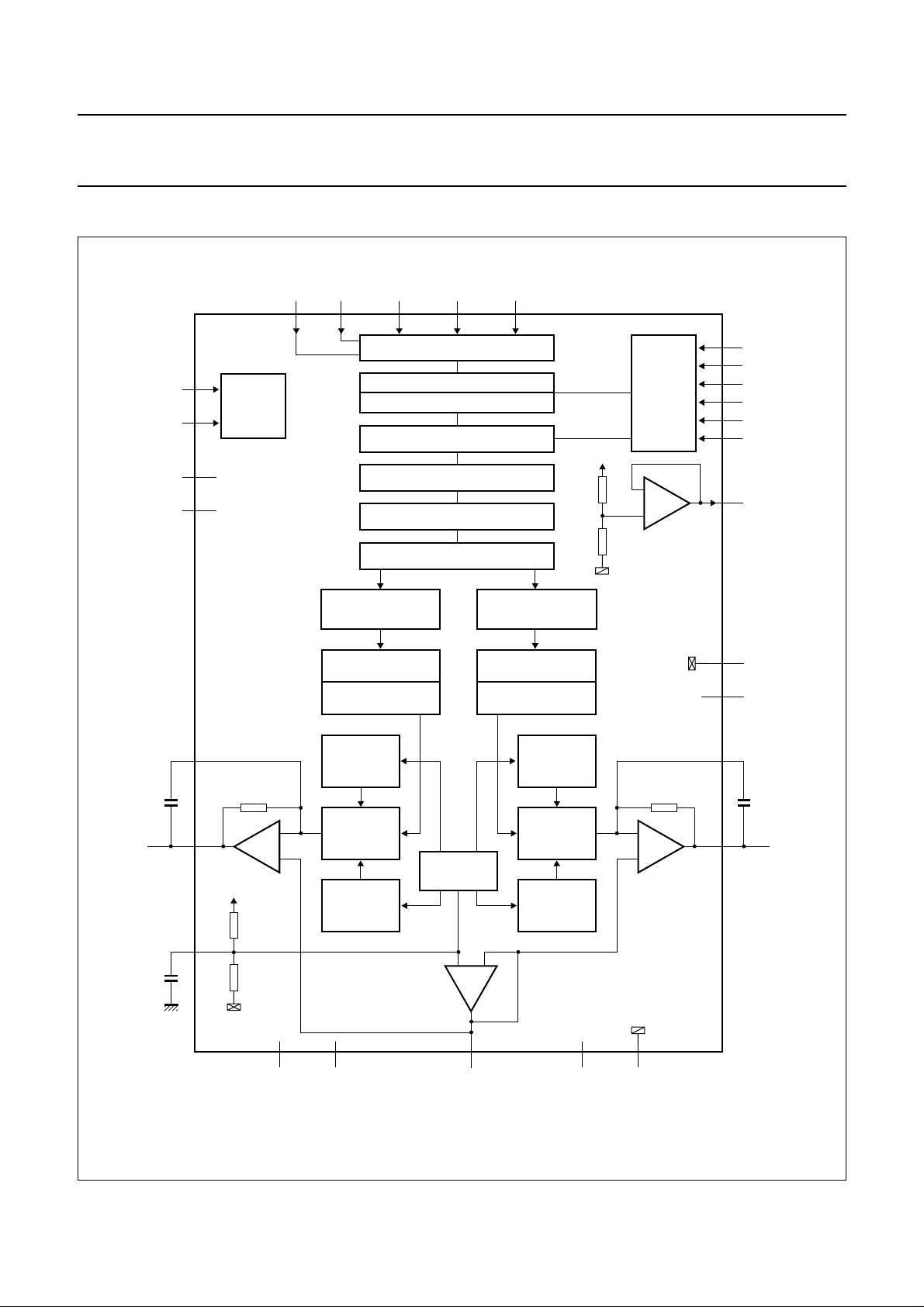
BLOCK DIAGRAM
handbook, full pagewidth
SYSCLK
CLSEL
MODE0
MODE1
12
TIMING
17
5
6
IF1 IF2 DATA WS BCK
13
14 9 8 7
SERIAL DATA INPUT
VOLUME CONTROL
SOFT MUTE CONTROL
SOUND CONTROL
FILTER STAGE 1
FILTER STAGE 2
LINEAR INTERPOLATOR
8 x OVERSAMPLING
(SAMPLE-AND-HOLD)
1 f
s
2 f
s
4 f
s
8 f
s
8 x OVERSAMPLING
(SAMPLE-AND-HOLD)
V
DDA
V
SSA
VOLUME
AND
SOUND
CONTROL
−
OP4
+
TDA1548T
16
MUTE
15
DEEM
22
AD3S
21
ADVC
20
ADBB
19
ADTR
18
AD
ref
1.8 nF
CEXT1
10
µF
V
VOL
V
ref
SSA
2nd ORDER
NOISE SHAPER
DATA
ENCODER
4
R
CONV1
1.2 kΩ 1.2 kΩ
3
V
DDA
25
V
SSA
OP1
6 kΩ
6 kΩ
V
−
+
SSO
16 (4-bit)
CALIBRATED
CURRENT
SOURCES
LEFT
OUTPUT
SWITCHES
16 (4-bit)
CALIBRATED
CURRENT
SINKS
V
DDO
REFERENCE
SOURCE
+
V
NOISE SHAPER
−
OP3
COM
2nd ORDER
DATA
ENCODER
16 (4-bit)
CALIBRATED
CURRENT
SOURCES
RIGHT
OUTPUT
SWITCHES
16 (4-bit)
CALIBRATED
CURRENT
SINKS
V
232281
DDA
R
CONV2
−
OP2
+
TDA1548T
24
V
SSA
11
10
26
27
MGC668
FILTCRFILTCL
VOR
V
SSD
V
DDD
1.8 nF
CEXT2
Fig.1 Block diagram.
1995 Nov 15 4
Philips Semiconductors Product specification
Bitstream continuous calibration filter-DAC
with headphone driver and DSP
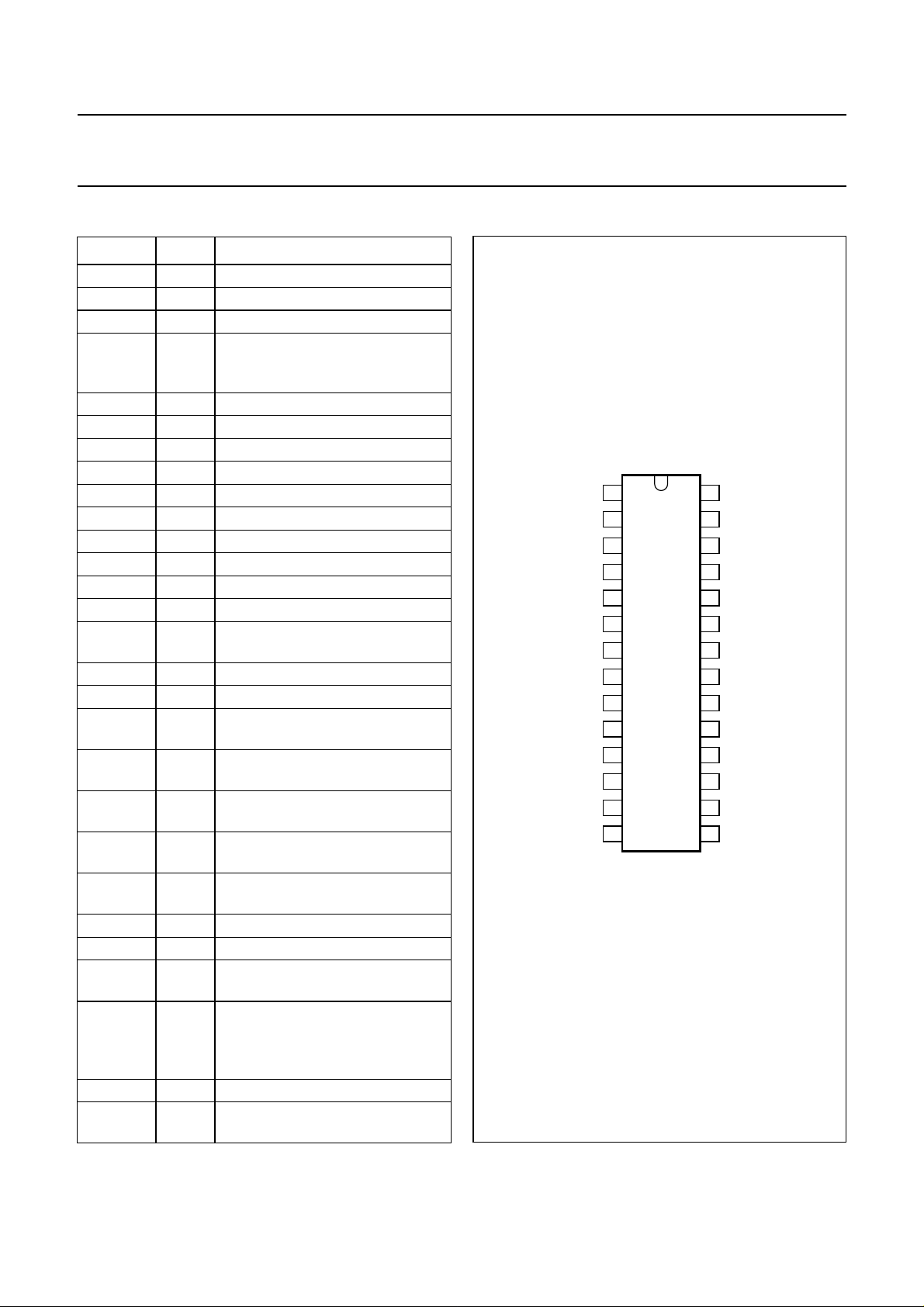
PINNING
SYMBOL PIN DESCRIPTION
V
SSO
V
COM
VOL 3 left channel audio voltage output
FIL TCL 4 capacitor for left channel first-order
MODE0 5 mode 0 selection pin
MODE1 6 mode 1 selection pin
BCK 7 bit clock input
WS 8 word select input
DATA 9 data input
V
DDD
V
SSD
SYSCLK 12 system clock 64f
IF1 13 input format selection 1
IF2 14 input format selection 2
DEEM 15 de-emphasis input (f
MUTE 16 soft-mute input (active HIGH)
CLSEL 17 system clock selection input
AD
ref
ADTR 19 analog sense input for treble
ADBB 20 analog sense input for bass boost
ADVC 21 analog sense input for volume
AD3S 22 3-position switch input for
V
DDA
V
SSA
V
ref
FILTCR 26 capacitor for right channel
VOR 27 right channel audio voltage output
V
DDO
1 operational amplifier ground
2 common output pin
filter function should be connected
between this pin and VOL (pin 3)
10 digital supply voltage
11 digital ground
, 256fs or 384f
s
= 44.1 kHz)
s
(active HIGH)
18 reference voltage output to
external potentiometer
setting
setting
control setting
flat/min/max setting
23 analog supply voltage
24 analog ground
25 internal reference voltage
(0.5V
DDA
typ)
first-order filter function should be
connected between this pin and
VOR (pin 27)
28 operational amplifier supply
voltage
s
handbook, halfpage
1
V
SSO
2
V
COM
3
VOL
BCK
4
5
6
7
FILTCL
MODE0
MODE1
TDA1548T
8
WS
9
DATA
10
V
DDD
11
V
SSD
IF1
IF2
12
13
14
MGC669
SYSCLK
Fig.2 Pin configuration.
TDA1548T
28
V
DDO
27
VOR
26
FILTCR
25
V
ref
24
V
SSA
23
V
DDA
22
AD3S
21
ADVC
20
ADBB
19
ADTR
18
AD
ref
17
CLSEL
16
MUTE
15
DEEM
1995 Nov 15 5

Philips Semiconductors Product specification
Bitstream continuous calibration filter-DAC
with headphone driver and DSP
FUNCTIONAL DESCRIPTION
The TDA1548T CMOS DAC incorporates an up-sampling
digital filter, a linear interpolator, a noise shaper,
continuous calibrated current sources and headphone
amplifiers. The 1fs input data is increased to an
oversampling rate of 64fs. This high-rate oversampling,
together with the 5-bit DAC, enables the filtering required
for waveform smoothing and out-of-band noise reduction
to be achieved by simple first-order analog post-filtering.
System clock and data input format
The TDA1548T accommodates slave mode only, this
means that in all applications the system devices must
provide the system clock. The system frequency is
selectable at pins CLSEL, MODE0 and MODE1
(see Table 1).
The TDA1548T supports the following data input modes
(see Table 2):
2
S-bus with data word length of up to 20 bits
I
LSB justified serial format with data word length of 16,
18 or 20 bits.
TDA1548T
For each multiplexed timeslot the full approximation cycle
is completed, immediately after which the next input will
start being sampled.
The time slot for one input lasts 64 steps at a step advance
rate of 8 × f
Because four inputs are multiplexed, the sample rate for
each analog input is 1.38 kHz.
A buffered version of an internally generated reference
voltage is available at output pin AD
internal AD derives from the same reference voltage, this
allows for optimum mapping of the external analog control
value onto the useful AD input voltage range. The idea is
to bias a potentiometer to AD
the input voltage between 0 V and AD
implemented to improve noise immunity of the AD in order
to prevent a stable setting of the potentiometer, to a point
near a quantization threshold, from producing two
alternating digital codes which could give rise to audible
volume or boost changes. An hysteresis of 1 LSB is
implemented digital. A shift in code must be at least 2 LSB
either up or down from the current value, otherwise the
internal digital code will remain at the current value.
, which amounts to 181 µs at fs= 44.1 kHz.
s
. Because the
ref
, using a wiper to control
ref
. Hysteresis is
ref
The input formats are illustrated in Fig.4. Left and right
data-channel words are time multiplexed.
Analog control of digital sound processing features
Digital sound processing settings are controlled via analog
sense inputs that translate an analog voltage from, for
example, a potentiometer wiper to a digital code, which is
then further translated internally to a set of coefficients for
either treble, bass boost or volume.
The analog input value is acquired by an internal 6-bit
ADC, sampling the three input pins ADVC, ADBB and
ADTR and the three-mode selection pin ADS3 (see
Section “Single pin three mode selection”) in a multiplexed
fashion. Sampling of the input voltage is performed by a
straight forward technique of linear approximation; from
the starting value of 0 V, an internal linear approximation
voltage is incremented periodically in steps of 1/66th of the
scale, with an internal comparator detecting when the
approximation value oversteps the input value. Tolerance
is built in at the top and bottom end of the scale by
dimensioning the resistive elements at the top and bottom
of the ladder equals 1R. Thus the ladder is built up of
64 elements of value R, two of value R, making a typical
quantization step size of approximately 1.5 V (AD
ref
)
divided-by-66 (amount of Rs), equals 22.7 mV.
S
INGLE PIN THREE MODE SELECTION
A special input pin AD3S (pin 22), controls the mode in
which the sound processing block operates. Not between
two but three modes; whether the DSP should follow the
AD inputs applying maximum effect, the minimum effect or
overrule the boost effects thereby resulting in a flat
frequency characteristic in the treble and bass boost
sections.
Internally the same AD is used to detect the input level
present at this pin as is used for the three sound control
pins. An internal bias circuit containing of two MOSTs
supplies a mid-range voltage so that this input can be
operated with a minimum of external components. A HIGH
or LOW input level is created by tying the pin to AD
ref
or
ground respectively, the intermediate value is achieved by
leaving the pin open-circuit.
Volume control
Since there is no headroom included into the sound control
section, the volume control precedes the sound control.
Full volume and neutral setting (flat) of the sound control
results in a full-scale output. Any tone boost will
immediately cause clipping, which can be avoided by
reducing the volume setting.
1995 Nov 15 6
 Loading...