

Philips TDA1547 Datasheet

INTEGRATED CIRCUITS
DATA SH EET
TDA1547
Dual top-performance bitstream
DAC
Product specification
File under Integrated Circuits, IC01
September 1991
Philips Semiconductors Product specification
Dual top-performance bitstream DAC TDA1547
FEATURES
• Top-grade audio performance
– very low harmonic distortion
– high signal-to-noise ratio
– wide dynamic range of approximately 108 dB
(not A-weighted)
• High crosstalk immunity
• Bitstream concept
– high over-sampling rate up to 192 f
– pulse-density modulation
– inherently monotonic
– no zero-crossing distortion
GENERAL DESCRIPTION
The TDA1547 is a dedicated one-bit digital-to-analog
converter to facilitate a high fidelity sound reproduction of
digital audio. The TDA1547 is extremely suitable for use in
high quality audio systems such as Compact Disc and
DAT players, or in digital amplifiers and digital signal
processing systems. The TDA1547 is used in combination
with the SAA7350 bitstream circuit, which includes the
s
third-order noise shaper. The excellent performance of the
SAA7350 and TDA1547 bitstream conversion system is
obtained by separating the noise shaping circuit and the
one-bit conversion circuit over two IC's, thereby reducing
the crosstalk between the digital and analog parts. The
TDA1547 one-bit converter is processed in BIMOS. In the
digital logic and drivers bipolar transistors are used to
optimize speed and to reduce digital noise generation. In
the analog part the bipolar transistors are used to obtain
high performance of the operational amplifiers. Special
layout precautions have been taken to achieve a high
crosstalk immunity. The layout of the TDA1547 has fully
separated left and right channels and supply voltage lines
between the digital and analog sections.
ORDERING INFORMATION
EXTENDED TYPE
NUMBER
TDA1547
Note
1. SOT-232-1; 1996 August 23.
(1)
PINS PIN POSITION MATERIAL CODE
PACKAGE
32 SDIL plastic SOT232A
September 1991 2
Philips Semiconductors Product specification
Dual top-performance bitstream DAC TDA1547
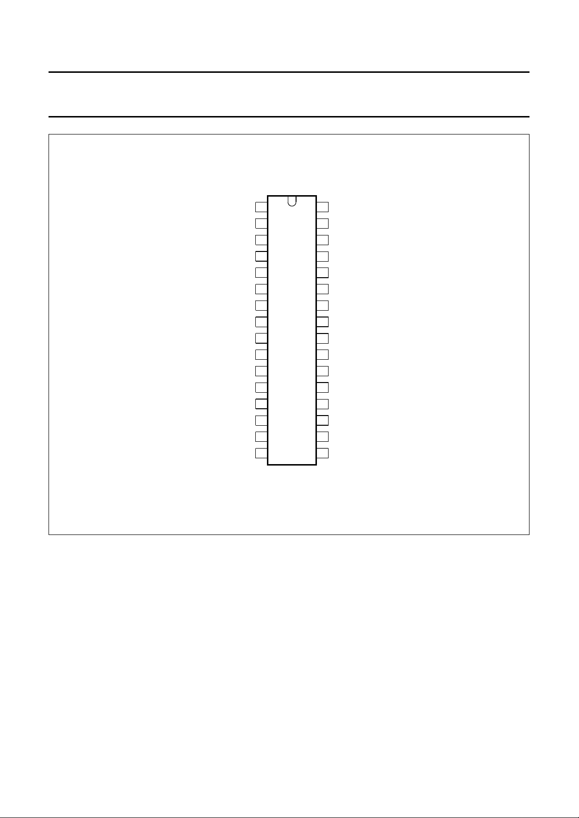
handbook, halfpage
AGND DAC R
DGND
V
DDD
IN R
n.c.
CLK R
V
DDD R
V
SSD R
V
ref R
– DAC R
+ DAC R
AGND R
n.c.
+ OUT R
– OUT R
V
SSA
1
2
3
4
5
6
7
8
9
10
11
12
13
14
15
16
TDA1547
MCD294
V
32
V
31
IN L
30
n.c.
29
CLK L
28
V
27
V
26
V
25
AGND DAC L
24
23
– DAC L
22
+ DAC L
21
AGND L
n.c.
20
19
+ OUT L
18
– OUT L
V
17
SUB
SSD
DDD L
SSD L
ref L
DDA
Fig.1 Pinning diagram.
September 1991 3

Philips Semiconductors Product specification
Dual top-performance bitstream DAC TDA1547
PINNING
SYMBOL PIN DESCRIPTION
DGND 1 0 V digital supply
V
DDD
IN R 3 serial one-bit data input for the right channel
n.c. 4 pin not connected; should preferably be connected to digital ground
CLK R 5 clock input for the right channel
V
DDD R
V
SSD R
V
ref R
AGND DAC R 9 0 V reference voltage for the right channel switched capacitor DAC; this pin should be
−DAC R 10 output from the right negative switched capacitor DAC; feedback connection for the right
+DAC R 11 output from the right positive switched capacitor DAC; feedback connection for the right
AGND R 12 0 V reference voltage for both right channel operational amplifiers
n.c. 13 pin not connected; should preferably be connected to analog ground
+OUT R 14 + output of the switched capacitor operational amplifier
−OUT R 15 − output of the switched capacitor operational amplifier
V
SSA
V
DDA
−OUT L 18 − output of the switched capacitor operational amplifier
+OUT L 19 + output of the switched capacitor operational amplifier
n.c. 20 pin not connected; should preferably be connected to analog ground
AGND L 21 0 V reference voltage for both left channel operational amplifiers
+DAC L 22 output from the left positive switched capacitor DAC; feedback connection for the left
−DAC L 23 output from the left negative switched capacitor DAC; feedback connection for left negative
AGND DAC L 24 0 V reference voltage for the left channel switched capacitor DAC; this pin should be
V
ref L
V
SSD L
V
DDD L
2 5 V digital supply for both channels
6 5 V digital supply for the right channel; this voltage determines the internal logic HIGH level
in the right channel
7 −3.5 V digital supply for the right channel; this voltage determines the internal logic LOW
level in the right channel
8 −4 V reference voltage for the right channel switched capacitor DAC
connected to analog ground
negative operational amplifier
positive operational amplifier
16 −5 V analog supply
17 5 V analog supply
positive operational amplifier
operational amplifier
connected to analog ground
25 −4 V reference voltage for the left channel switched capacitor DAC
26 −3.5 V digital supply for the left channel; this voltage determines the internal logic LOW level
in the left channel
27 5 V digital supply for the left channel; this voltage determines the internal logic HIGH level in
the left channel
September 1991 4
Philips Semiconductors Product specification
Dual top-performance bitstream DAC TDA1547
SYMBOL PIN DESCRIPTION
CLK L 28 clock input for the left channel
n.c. 29 pin not connected; should preferably be connected to digital ground
IN L 30 serial one-bit data input for the left channel
V
SSD
V
SUB
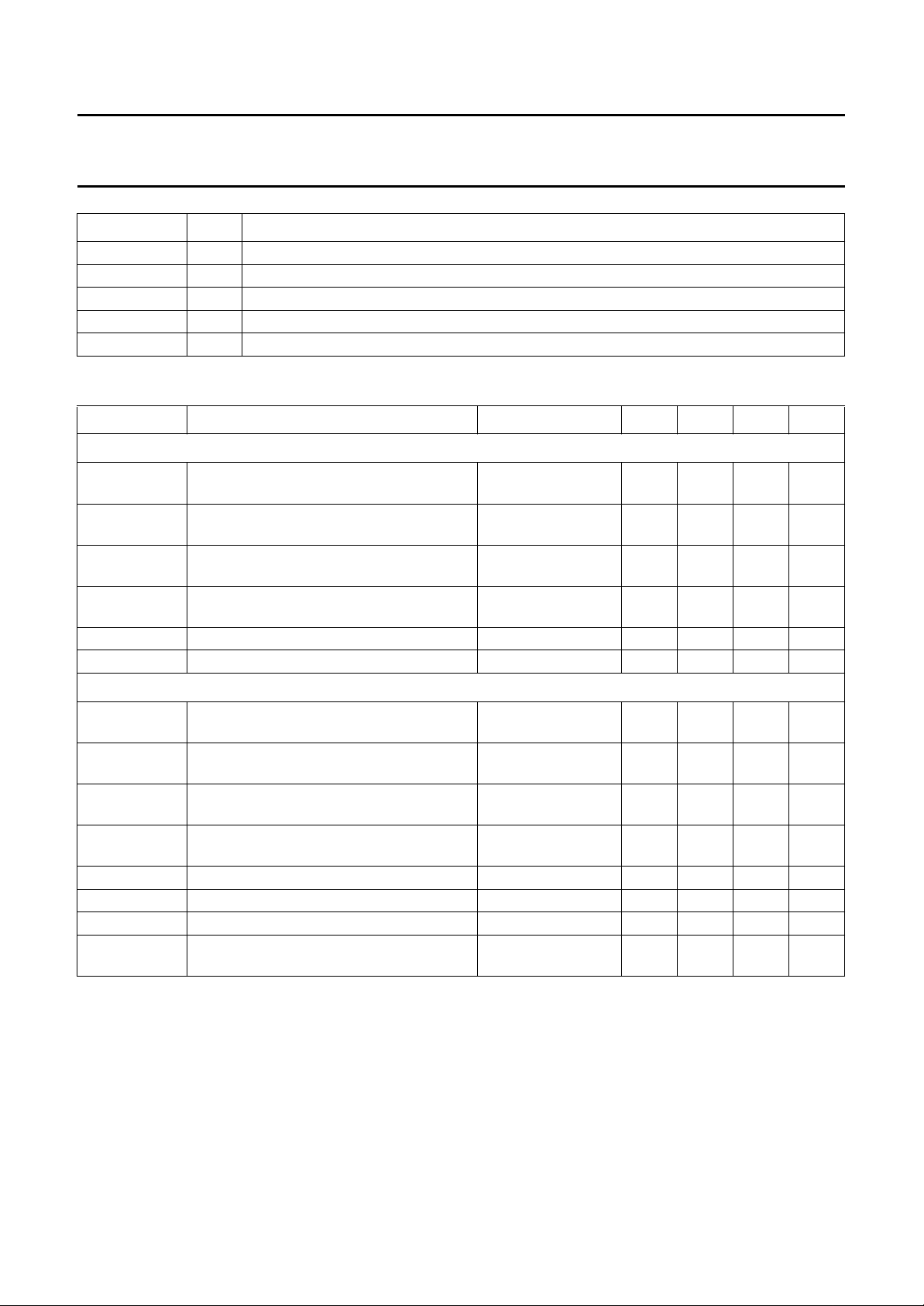
QUICK REFERENCE DATA
SYMBOL PARAMETER CONDITION MIN TYP MAX UNIT
Supply voltages
V
DDD L. R
V
DDD
V
SSD L. R
V
SSD
V
DDA
V
SSA
Supply current
I
DDD L. R
I
DDD
I
SSD L. R
I
SSD
I
DDA
I
SSA
P
tot
V
OUT(RMS)
31 −5 V digital supply for both channels
32 −5 V substrate voltage
positive digital supply voltage for one
4.5 5.0 5.5 V
channel; pins 27 and 6
digital supply voltage for both channels;
4.5 5.0 5.5 V
pin 2
negative digital supply voltage for one
−4.0 −3.5 −3.0 V
channel; pins 26 and 7
negative digital supply voltage for both
−5.5 −5.0 −4.5 V
channels; pin 31
positive analog supply voltage; pin 17 4.5 5.0 6 V
negative analog supply voltage; pin 16 −6.0 −5.0 −4.5 V
positive digital supply current for one
− 0.1 − mA
channel; pins 27 and 6
digital supply current for both channels;
− 29.0 − mA
pin 2
negative digital supply current for one
−−0.1 − mA
channel; pins 26 and 7
negative supply current for both channels;
−−28.0 − mA
pin 31
positive analog supply current; pin 17 − 51.0 − mA
negative analog supply current; pin 16 −−51.0 − mA
total power dissipation − 800 − mW
output voltage (RMS value) f
= 8.46 MHz;
CLK
0.85 1.0 1.15 V
notes 1 and 2
September 1991 5
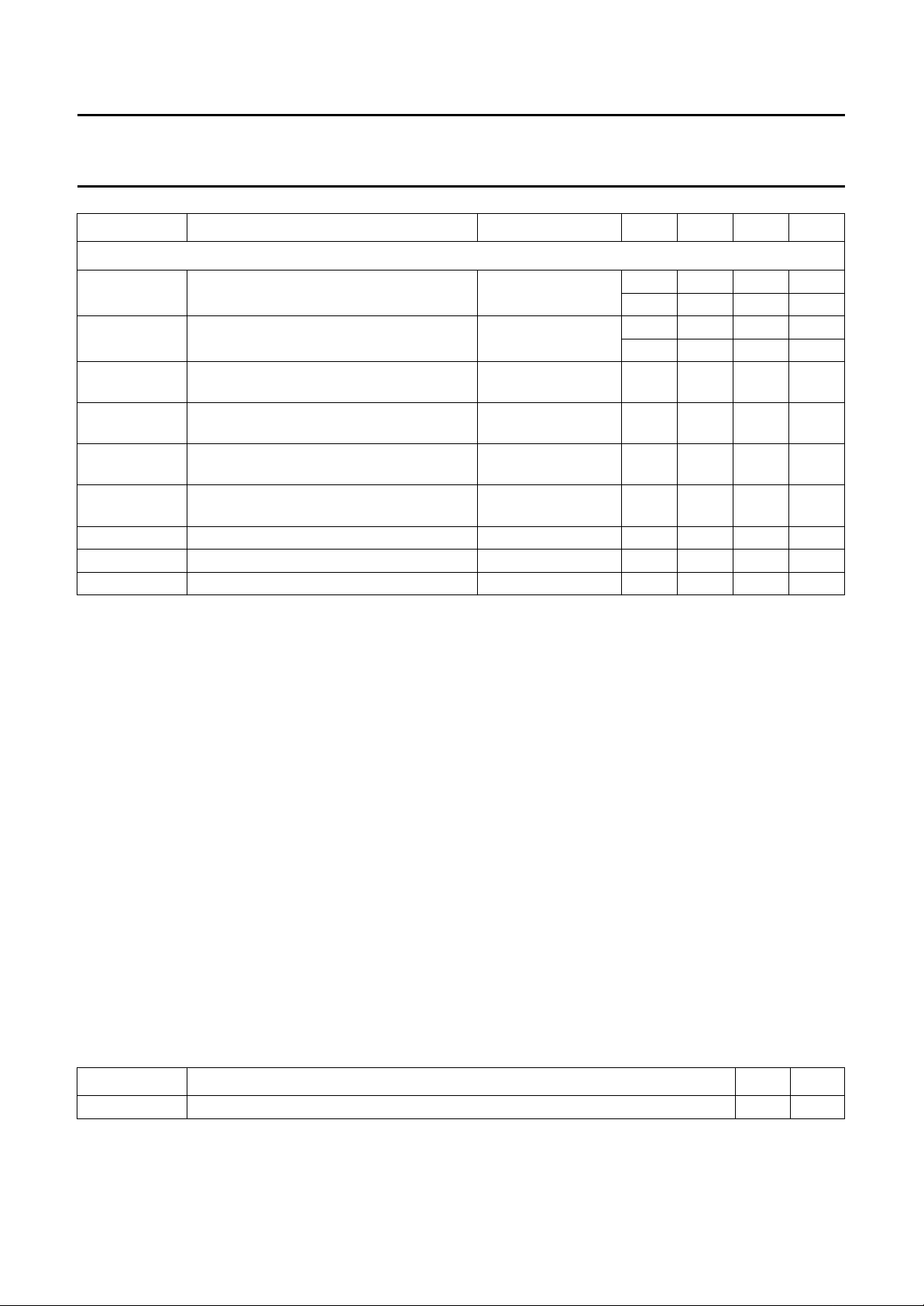
Philips Semiconductors Product specification
Dual top-performance bitstream DAC TDA1547
SYMBOL PARAMETER CONDITION MIN TYP MAX UNIT
Supply current
(THD + N)/S THD + Noise; 0 dB 1 kHz; notes 2 and 3 −−101 −96 dB
− 0.0009 0.0016 %
(THD + N)/S THD + Noise; 0 dB f = 20 Hz to 20 kHz; −−101 - dB
notes 2 and 4 − 0.0009 - %
(THD + N)/S THD + Noise; −20 dB f = 1 kHz;
notes 2 and 3
(THD + N)/S THD + Noise; −60 dB f = 1 kHz;
notes 2 and 3
S/N signal-to-noise ratio pattern 0101..;
notes 2 and 5
S/N signal-to-noise ratio; “A”-weighting pattern 0101..;
notes 2 and 5
f
CLK
maximum clock frequency −−10 MHz
α channel separation f = 1 kHz 101 115 − dB
T
amb
operating ambient temperature −20 − 70 °C
Notes to the quick reference data
1. Output level tracks linearly with both the clock frequency and the reference voltage (V
2. Device measured in differential mode with external components as shown in Fig.5.
3. Measured with a one-bit data signal generated by the SAA7350 from an 8 fs (352.8 kHz), 20-bit, 1 kHz digital
sinewave. Measured over a 20 Hz to 20 kHz bandwidth.
4. Measured with a one-bit data signal generated by the SAA7350 from an 8 fs (352.8 kHz), 20-bit, 20 Hz to 20 kHz
digital sinewave. Measured over a 20 Hz to 20 kHz bandwidth.
5. The specified signal-to-noise ratio includes noise introduced by the application components as shown in Fig.5.
−−88 −84 dB
−−48 −44 dB
109 111 − dB
− 113 − dB
ref L
or V
ref R
).
FUNCTIONAL DESCRIPTION
Both channels are completely separated to reach the desired high crosstalk suppression level.
Each channel consists of the following functional parts:
− One-bit input, which latches the incoming data to the system clock.
− Switch driver circuit, which generates the non-overlapping clock- and data-signals that control the DAC switched
capacitor networks.
− Switched capacitor network, this forms the actual DAC function, it supplies charge packets to the low-pass filter,
under control of the incoming one-bit code.
− Two high performance operational amplifiers, that perform the charge packet to voltage conversion and deliver a
differential output signal. The first pole of the low-pass filter is built around them.
THERMAL RESISTANCE
SYMBOL PARAMETER MAX. UNIT
R
th j-a
from junction to ambient 60 K/W
September 1991 6
 Loading...