

Philips TDA1546T Datasheet
INTEGRATED CIRCUITS
DATA SH EET
TDA1546T
Bitstream Continuous Calibration
DAC with digital sound processing
(BCC-DAC)
Preliminary specification
File under Integrated Circuits, IC01
Philips Semiconductors
January 1995

Philips Semiconductors Preliminary specification
Bitstream Continuous Calibration DAC with
digital sound processing (BCC-DAC)
CONTENTS
1 FEATURES
1.1 Easy application
1.2 High performance
1.3 Digital sound processing features
1.3.1 Volume control features
1.3.2 Sound processing features
1.3.3 Sound monitor features
2 ORDERING INFORMATION
3 QUICK REFERENCE DATA
4 GENERAL DESCRIPTION
5 BLOCK DIAGRAM
6 PINNING
7 FUNCTIONAL DESCRIPTION
7.1 Clock generation and distribution
7.2 Power-on reset
7.3 Microprocessor interface
7.3.1 Address mode
7.3.2 Data transfer mode
7.3.3 Organization and programming of the internal
register file
7.3.3.1 Volume control register bits: BAL3 to BAL0 and
BAR3 to BAR0
7.3.3.2 Volume control register bits: VC7 to VC0 and
FT3 to FT0
7.3.3.3 Volume control register bit: MUTE
7.3.3.4 Volume control register bit: RUNFA
7.3.3.5 Sound monitor register bits: FP2 to FP0
7.3.3.6 Sound monitor register bits: OVER3 to OVER0
7.3.3.7 Sound monitor register bits: SIL3 to SIL0 and
SILT3 to SILT0
7.3.3.8 Sound monitor register bit SPOS
7.3.3.9 Sound processing register bit: DSS
7.3.3.10 Sound processing register bits: SCT3 to SCT0
7.3.3.11 Sound processing register bits: SCB3 to SCB0
7.3.3.12 Sound processing register bits: SCBB3 to
SCBB0
7.3.3.13 Sound processing register bits: DEMC1 and
DEMC0
7.3.3.14 Sound processing register bit: DSM
7.3.3.15 Miscellaneous register bits: ED3 to ED0
7.3.3.16 Miscellaneous register bits: EA2 to EA0
7.3.3.17 Miscellaneous register bits: INS1 and INS0
7.3.3.18 Miscellaneous register bits: PVIV1, PVIV0 and
PINM1, PINM0
7.3.3.19 Miscellaneous register bit: CLRM
7.3.3.20 Miscellaneous register bits: OUTS1 and
OUTS0
7.3.3.21 Miscellaneous register bit: LONLY
7.3.3.22 Miscellaneous register bits: FSO1, FSO0, TRI,
7.4 Multiple format input interface
7.4.1 Synchronization
7.5 Normal-speed mode
7.6 Double-speed mode
7.6.1 Double-speed mode features
7.6.2 Low-power option using double-speed mode
7.7 Volume control features
7.7.1 Digital balance
7.7.2 Digital volume control with fade function
7.7.3 Digital soft-mute
7.7.4 Scaling and polarity of the digital up-sampling
7.8 Sound processing related features
7.8.1 De-emphasis filter
7.8.2 Treble
7.8.3 Bass
7.8.4 Bass boost
7.8.5 Digital dynamic bass boost, digital loudness
7.8.6 Digital speaker system mode
7.9 Sound monitor block
7.9.1 Spectrum analyzer
7.9.2 dB converter
7.9.3 Peak detection
7.9.4 Silence detection
7.9.5 Overload detection
7.9.6 Versatile outputs
7.10 Noise shaper
7.11 Continuous calibration digital-to-analog
7.12 Operational amplifiers
7.13 Internal reference circuitry
8 LIMITING VALUES
9 THERMAL CHARACTERISTICS
10 QUALITY SPECIFICATION
11 CHARACTERISTICS
12 ANALOG CHARACTERISTICS
TDA1546T
ACDT, DCDT, CLKIV, CLKON, DYC1 and
DYC0
filter
and other dynamic applications of tone control
converter
January 1995 2

Philips Semiconductors Preliminary specification
Bitstream Continuous Calibration DAC with
digital sound processing (BCC-DAC)
13 APPLICATION INFORMATION
13.1 Digital filter characteristics (theoretical values)
13.2 Example application circuit
14 PACKAGE OUTLINE
15 SOLDERING
15.1 Plastic small-outline packages
15.1.1 By wave
15.1.2 By solder paste reflow
15.1.3 Repairing soldered joints (by hand-held
soldering iron or pulse-heated solder tool)
16 DEFINITIONS
17 LIFE SUPPORT APPLICATIONS
18 PURCHASE OF PHILIPS I2C COMPONENTS
TDA1546T
January 1995 3

Philips Semiconductors Preliminary specification
Bitstream Continuous Calibration DAC with
digital sound processing (BCC-DAC)
1 FEATURES
1.1 Easy application
• Voltage output 1.5 V (RMS)
• Operational amplifiers and cascaded 4-stage digital FIR
filter integrated
• Master and slave mode clock system with selectable
system clock (f
• I2S-bus serial input format or Japanese 16, 18 or 20 bits
serial input mode
• All features are accessible under remote control
• Simple 3-line serial microcontroller command interface
• Power-on reset
• 28 lead small outline package.
1.2 High performance
• Superior signal-to-noise ratio
• Low total harmonic distortion
• Wide dynamic range
• No zero crossing distortion
• Continuous calibration digital-to-analog conversion
combined with noise shaping techniques
• Second-order noise shaper
• 128 times oversampling in normal-speed mode
• 64 times oversampling in double-speed mode.
1.3 Digital sound processing features
1.3.1 V
• Smoothed transitions before and after digital mute (soft
mute)
• Fade function: duration-programmable (6 ms to 22.4 s
at 44.1 kHz) digital volume control (attenuation as well
as gain): +6 dB to −90 dB in steps of 0.375 dB with
automatic soft mute
• Digital balance: 0 dB to −22.5 dB in steps of −1.5 dB
(maximum overall attenuation combined with volume
control: −90 dB)
OLUME CONTROL FEATURES
) 256fs or 384f
sys
s
TDA1546T
1.3.2 S
• Digital de-emphasis filter for three sample rates (32 kHz,
44.1 kHz or 48 kHz)
• Digital treble: −10.5 dB to +12 dB at 20 kHz; 16 steps
spaced at 1.5 dB
• Digital bass: −9 dB to +13.5 dB at 20 Hz; 16 steps
spaced at 1.5 dB
• Distortion-free digital dynamic bass boost: 0 dB to
+37 dB at 10 Hz; 15 steps spaced at 2 dB
• Can be used for loudness or dynamic digital bass boost
• Double-speed mode (e.g. for high-speed dubbing)
• Pseudo double-speed mode (for power saving
application)
• Digital speaker system mode including digital crossover
filter.
1.3.3 S
• Spectrum analyzer for seven different frequency ranges
• Digital silence detection. Level (−48 dB to∞dB, in steps
of 3 dB) and duration (200 ms to 3.2 s, in steps of
200 ms at 44.1 kHz) programmable. Output via versatile
pins.
• Peak level detection and readout to microcontroller
(dB linear, 0 dB to −90 dB in steps of 1.5 dB)
• Digital overload detection. Level-programmable (dB
linear, −1.5 dB to−46.5 dB, in steps of 3 dB). Output via
versatile pins.
• Digital spectrum analyzer by combination of peak
detection and 7-band selective filter
• Optional combination spectrum analyzer and overload
detection for frequency-dependent overload detection.
OUND PROCESSING FEATURES
OUND MONITOR FEA TURES
2 ORDERING INFORMATION
TYPE
NUMBER
TDA1546T SO28 plastic small outline package; 28 leads; body width 7.5 mm SOT136-1
January 1995 4
NAME DESCRIPTION VERSION
PACKAGE
Philips Semiconductors Preliminary specification
Bitstream Continuous Calibration DAC with
TDA1546T
digital sound processing (BCC-DAC)
3 QUICK REFERENCE DATA
SYMBOLS PARAMETER CONDITIONS MIN. TYP. MAX. UNIT
V
DD
I
DDD
I
DDA
I
DDO
I
DDX
V
FS(rms)
(THD+N)/S total harmonic distortion
S/N signal-to-noise ratio at
t
dg
BR input bit rate at data input fs= 48 kHz;
f
sys
TC
FS
T
amb
supply voltage note 1 3.8 5.0 5.5 V
digital supply current note 2 − 40 − mA
analog supply current note 2 − 5.5 − mA
operational amplifier
note 2 − 6.5 − mA
supply current
clock circuitry supply
note 2 − 1 − mA
current
full-scale output voltage
VDD= 5 V 1.425 1.5 1.575 V
(RMS value)
at 0 dB signal level −−88 −81 dB
plus noise-to-signal ratio
at −60 dB signal level;
− 0.004 0.009 %
−−44 −40 dB
A-weighted
A-weighted; at code
bipolar zero
00000H
group delay fs= sample rate;
normal-speed
100 108 − dB
−−s
24
-----f
s
−− 3.072 Ms
normal-speed
fs= 48 kHz;
−− 6.144 Ms
double-speed
system clock frequency 6.4 − 18.432 MHz
full-scale temperature
−±100× 10−6−
coefficient at analog
outputs (VOL and VOR)
operating ambient
−20 − +70 °C
temperature
−1
−1
Notes
1. All V
and VSS pins must be connected to the same supply or ground respectively.
DD
2. Measured at input code 00000H and VDD=5V.
January 1995 5
Philips Semiconductors Preliminary specification
Bitstream Continuous Calibration DAC with
digital sound processing (BCC-DAC)
4 GENERAL DESCRIPTION
The TDA1546T is the first Bitstream Continuous
Calibration digital-to-analog converter (BCC-DAC) to
feature unique signal processing functions. In addition to
the basic functions of digital filtering and digital-to-analog
conversion, it offers such advanced digital signal
processing functions as volume control, tone control, bass
boost, peak or spectrum analyzer readout and many more
convenient functions. The digital processing features are
of high sound quality due to the wide dynamic range of the
bitstream conversion technique.
2
The TDA1546T accepts I
word lengths of up to 20 bits and various Japanese serial
data input formats with word lengths of 16, 18 and 20 bits.
The circuit can operate as a master or slave with different
system clocks (256fs or 384fs) and is therefore, eminently
suitable for use in various applications such as DCC, CD,
DAT and MD.
S-bus data input formats with
TDA1546T
The range of applications is further extended by an
incorporated Digital Speaker System mode (DSS) with
digital crossover filter.
Four cascaded FIR filters and a sample-and-hold function
increase the oversampling rate from 1f
(384fssystem clock) or 128fs (256fs system clock).
A second-order noise shaper converts this oversampled
data to a bitstream for the 5-bit DACs.
The DACs are of the continuous calibration type and
incorporate a special data coding technique, which
contributes to a high signal-to-noise ratio and dynamic
range.
On-board amplifiers convert the output current to a voltage
signal capable of driving a line output. Externally
connected capacitors perform the required first-order
filtering. Additional post filtering is not required.
to 96f
s
s
Fig.1 Digital audio reconstruction system using the TDA1546T.
January 1995 6
Philips Semiconductors Preliminary specification
Bitstream Continuous Calibration DAC with
digital sound processing (BCC-DAC)
5 BLOCK DIAGRAM
handbook, full pagewidth
VERS1
VERS0
SPECTRUM ANALYSER
dB CONVERTER
SILENCE
DETECTION
21
VERSATILE
20
OUTPUT
BCK5WS6DATA
4
PEAK
DETECTION
OVERLOAD
DETECTION
SOURCE
SELECTION
MULTIPLE FORMAT
INPUT INTERFACE
DE-EMPHASIS
VOLUME CONTROL
BALANCE
SOFT MUTE
TONE CONTROL 1
BASS
TONE CONTROL 2
TREBLE
TONE CONTROL 3
BASS BOOST
CKSL
7
CRYSTAL
OSCILLATOR
CLOCK
GENERATION
AND
DISTRIBUTION
TDA1546T
12
XTAL1
13
XTAL2
16
CDEC
14
V
DDX
15
V
SSX
10
V
DDD
9
V
SSD
TEST1
TEST2
1 nF
C
EXT1
1 µF
V
V
GND
OL
FIR FILTER
3
11
23FILTCL
2.2 kΩ
22
26
ref
TDA1546T
LINEAR INTERPOLATOR 8f to 16f
6 x OVERSAMPLING (SAMPLE-AND-HOLD)
SECOND ORDER NOISE SHAPER
DATA ENCODER
LEFT OUTPUT SWITCHES
16 (4-bit)
R
CONV1
V
27
SSO
CALIBRATED
CURRENT
SOURCES
16 (4-bit)
CALIBRATED
CURRENT
28
V
DDO
SINKS
STAGE 1:1f to 2f
STAGE 2:2f to 4f
STAGE 3:4f to 8f
ss
REFERENCE
SOURCE
ss
FIR FILTER
ss
FIR FILTER
s
s
LINEAR INTERPOLATOR 8f to 16f
6 x OVERSAMPLING (SAMPLE-AND-HOLD)
SECOND ORDER NOISE SHAPER
RIGHT OUTPUT SWITCHES
16 (4-bit)
CALIBRATED
CURRENT
SOURCES
16 (4-bit)
CALIBRATED
CURRENT
SINKS
MICROCONTROLLER
INTERFACE
DATA ENCODER
1
V
DDA
ss
R
V
SSA
CONV2
2.2 kΩ
OP1OP1
2
8
19
18
17
24 FILTCR
25
MLC782
POR
L3DATA
L3CLK
L3MODE
V
OR
C
1 nF
EXT2
Fig.2 Block diagram.
January 1995 7
Philips Semiconductors Preliminary specification
Bitstream Continuous Calibration DAC with
digital sound processing (BCC-DAC)
6 PINNING
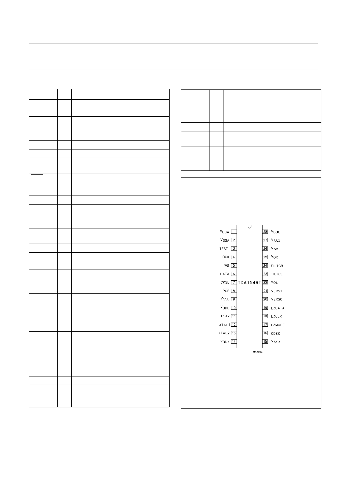
SYMBOL PIN DESCRIPTION
V
DDA
V
SSA
TEST1 3 Test input 1. This pin should be
BCK 4 Bit clock input
WS 5 Word select input
DATA 6 Data input
CKSL 7 System clock frequency selection
POR 8 Power-on reset (active LOW). Internal
V
SSD
V
DDD
TEST2 11 Test input 2. This pin should be
XT AL1 12 Crystal oscillator input in master mode
XT AL2 13 Crystal oscillator drive output to crystal
V
DDX
V
SSX
CDEC 16 System clock output
L3MODE 17 Identification of the L3-bus operation
L3CLK 18 Bit clock for synchronization of
L3DATA 19 Bidirectional data line intended for
VERS0 20 Versatile output 0 for silence or
VERS1 21 Versatile output 1 for silence or
V
OL
FILTCL 23 Capacitor for left channel first-order
1 Analog supply voltage
2 Analog ground
connected to ground.
input
pull-up resistor allows timed operation
in combination with external capacitor.
9 Digital ground
10 Digital supply voltage
connected to ground.
or external clock input in slave mode
14 Crystal oscillator supply voltage
15 Crystal oscillator ground
mode
microcontroller data transfer
control data from the microcontroller
and peak data from the TDA1546T
overload detection. Can be used to
drive an LED.
overload detection. Can be used to
drive an LED.
22 Left channel audio voltage output
filter function should be connected
between this pin and V
(pin 22).
OL
TDA1546T
SYMBOL PIN DESCRIPTION
FILTCR 24 Capacitor for right channel first-order
filter function should be connected
between this pin and VOR (pin 25).
V
V
V
V
OR
ref
SSO
DDO
25 Right channel audio voltage output
26 Decoupling pin for internal reference
voltage,1⁄2V
DDA
(typ)
27 Internal operational amplifier ground
28 Internal operational amplifier supply
voltage
Fig.3 Pin configuration.
January 1995 8
Philips Semiconductors Preliminary specification
Bitstream Continuous Calibration DAC with
digital sound processing (BCC-DAC)
7 FUNCTIONAL DESCRIPTION
The TDA1546T CMOS digital-to-analog bitstream
converter incorporates an up-sampling digital filter and
noise shaper which increase the oversample rate of 1f
input data to 128fs in the normal-speed mode. This
high-rate oversampling, together with the 5-bit DAC,
enables the filtering required for waveform smoothing and
out-of-band noise reduction to be achieved by simple
first-order analog post-filtering.
In the double-speed mode, the input sample frequency is
twice that of the normal-speed mode, as is the signal
bandwidth. The TDA1546T is able to distinguish between
the two modes (by means of a special programming bit),
so that in the double-speed mode, only half the amount of
oversampling is applied, and digital filtering is applied over
double the bandwidth compared to normal-speed. Thus in
the double-speed mode, the input sample rate of 1fs input
data is up-sampled by a factor 64f
, achieving the same
s
absolute output sample frequency as in normal-speed
mode.
In the block diagram, Fig.2, a general subdivision into main
functional Sections is illustrated. The actual signal
processing takes place in the digital signal processing
block. The two blocks named microcontroller interface and
clock generation and distribution fulfil a general auxiliary
function to the audio data processing path. The
microcontroller interface provides access to all the blocks
that require, or allow, configuration or selection and
processes the data readout from the peak detection block,
all via a simple three-line interface. The clock generation
and distribution section, which is driven by the external
system clock or crystal oscillator, provides the data
processing blocks with time bases and controls the system
mode dependent frequency settings. The following
sections give detailed explanations of the operation of
each block and their setting options processed by the
microcontroller interface, the use of the microcontroller
interface and of the operation of the clock section with its
various system settings.
s
TDA1546T
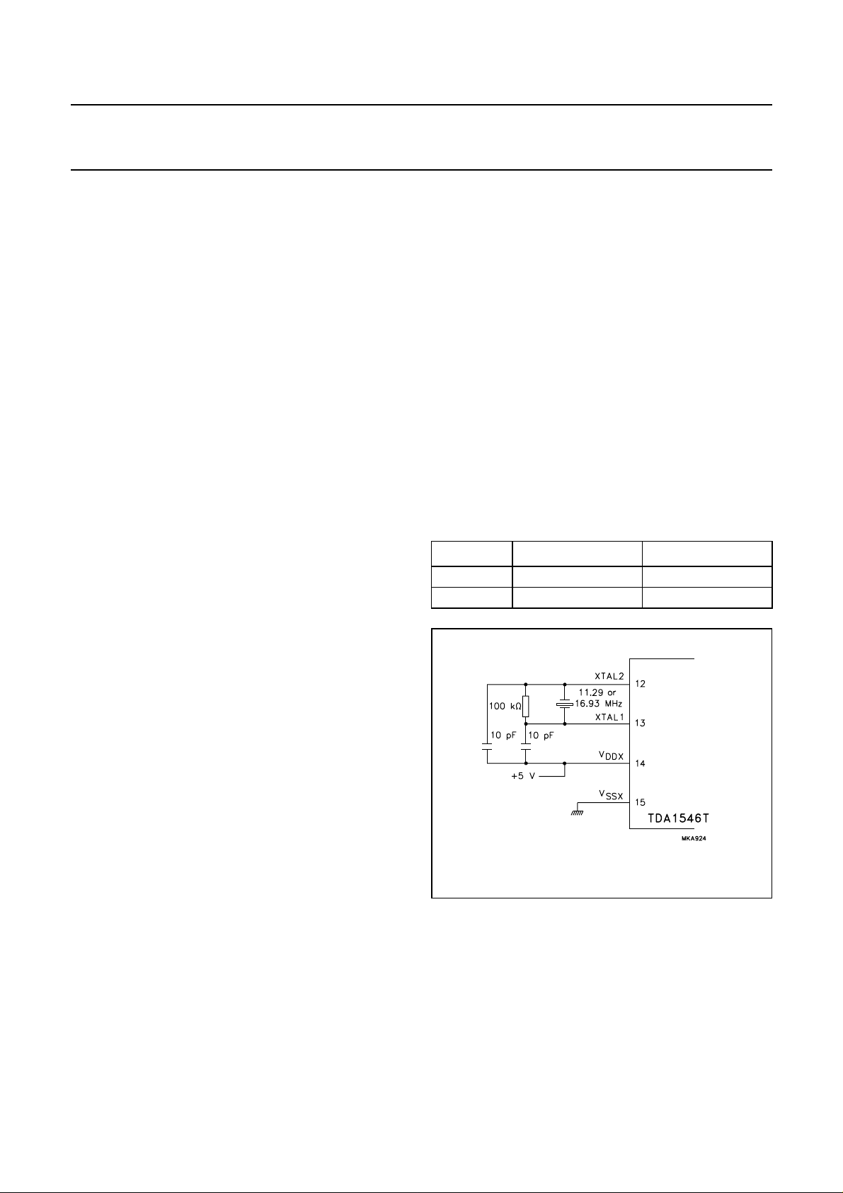
7.1 Clock generation and distribution
The TDA1546T has an internal clock generator that may
be used by connecting a crystal of 11.2896 MHz (256f
16.9344 MHz (384fs) between pins XTAL1 and XTAL2.
This mode is used when the TDA1546T is the master in
the system. The circuit diagram of Fig.4 shows the typical
connection of the external oscillator circuitry for master
mode operation.
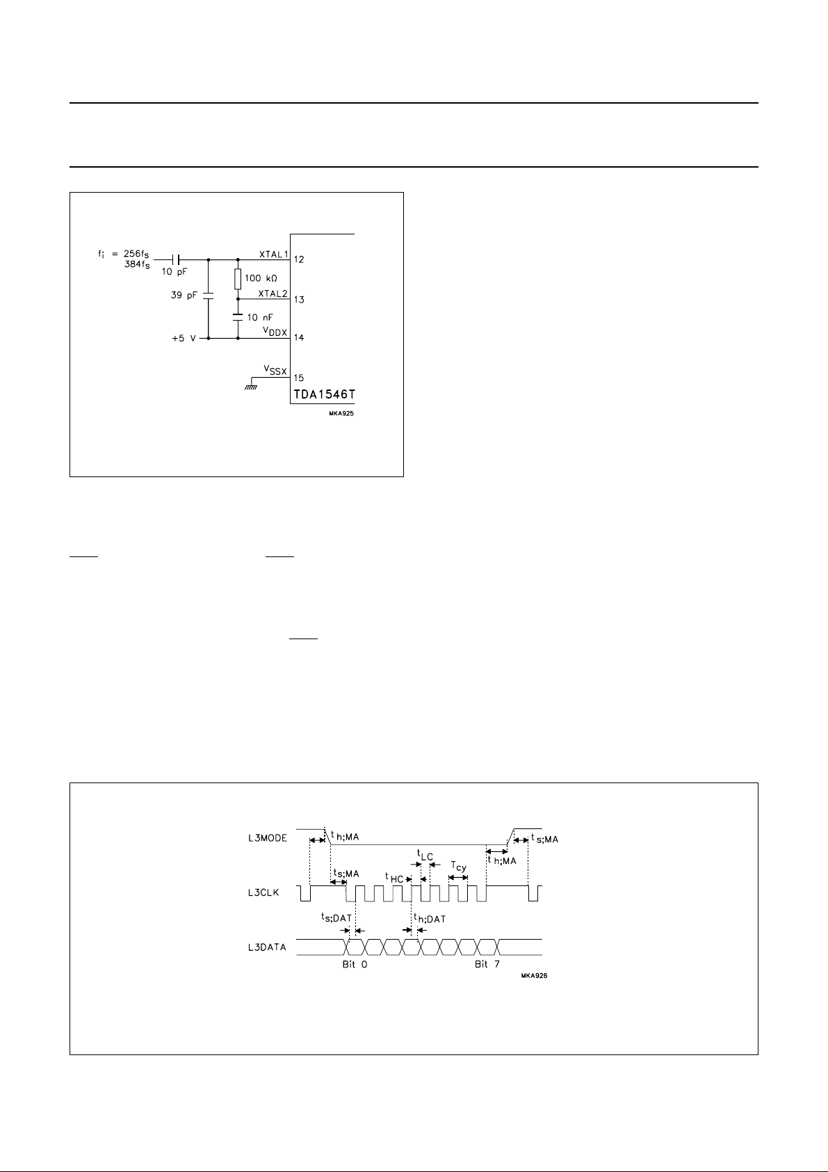
Alternatively, the TDA1546T can also operate in slave
mode. Figure 5 shows how to connect for slave mode
operation. In this mode, pin XTAL1 receives an input clock
of 256 or 384f
(fs= 32, 44.1 or 48 kHz) and voltage levels
s
of 0 V to 5 V by AC coupling and attenuation.
The CDEC output (pin 16) contains a buffered version of
the system clock for external use. The clock selection pin
CKSL is used to select between system clock frequency
ratios. Its effect is shown in Table 1.
Table 1 System clock selection
PIN CKSL SYSTEM CLOCK CDEC OUTPUT
0 256f
1 384f
s
s
256f
384f
Fig.4 External crystal oscillator circuit.
) or
s
s
s
January 1995 9
Philips Semiconductors Preliminary specification
Bitstream Continuous Calibration DAC with
digital sound processing (BCC-DAC)
Fig.5 External clock input connection.
7.2 Power-on reset
The internal register file of the TDA1546T is initialized by a
power-on reset sequence which can be instigated via the
POR input pin 8. A LOW input on POR causes the reset
sequence to be active. This input has an internal
resistance to VDD to allow for passive use with only an
external capacitor connected between this pin and ground.
For correct detection by the TDA1546T internal controller,
the system clock must be running, andPOR should remain
LOW for at least one audio sample period before being
returned HIGH. Following detection another audio sample
period is needed to complete the initialization procedure,
after which the values of the various control bits in the
internal register file are at their predefined initial values
(see Section 7.3).
TDA1546T
7.3 Microprocessor interface
The exchange of data and control information between the
TDA1546T and a microcontroller is accomplished through
a serial hardware interface comprising the following pins:
L3DATA: microcontroller interface bidirectional data
line.
L3CLK: microcontroller interface clock line.
L3MODE microcontroller interface mode line.
Information transfer through the microcontroller bus is
organized according to the so-called ‘L3’ format, in which
two different modes of operation can be distinguished;
address mode and data transfer mode.
The address mode is required to select a device
communicating via the L3-bus and to determine the
direction of data transfer in data transfer mode. Data
transfer for the TDA1546T can be in two directions, input
to the TDA1546T to program its sound processing and
other functional features, and output from the TDA1546T
for transfer of audio peak data, which it has acquired and
processed, to the system microcontroller.
7.3.1 A
The address mode is used to select a device for
subsequent data transfer and to define the direction of that
transfer as well as the source or destination registers. The
address mode is characterized by L3MODE being LOW
and a burst of 8 clock pulses on L3CLK, accompanied by
8 data bits. The fundamental timing is shown in Fig.6.
DDRESS MODE
Fig.6 Timing address mode.
January 1995 10
Philips Semiconductors Preliminary specification
Bitstream Continuous Calibration DAC with
digital sound processing (BCC-DAC)
Data bits 0 to 1 indicate the type of the subsequent data
transfer as shown below in Table 2. The direction of the
channel status and user data transfers depends on the
transmit/receive mode.
Table 2 Selection of data exchange
(1)
BIT 1
X 0 data to TDA1546T input
X 1 data from
Note
1. Where X = don't care.
Data bits 2 to 7 represent a 6-bit device address, with bit 7
being the MSB and bit 2 the LSB. The address of the
BIT 0 TRANSFER DIRECTION
output
TDA1546T
TDA1546T
TDA1546T is 000100 (bit 7 to bit 2). In the event that the
TDA1546T receives a different address, it immediately
3-states the L3DATA pin and deselects its microcontroller
interface logic. A dummy address of 000000 is defined for
the deselection of all devices that are connected to the
serial microcontroller bus.
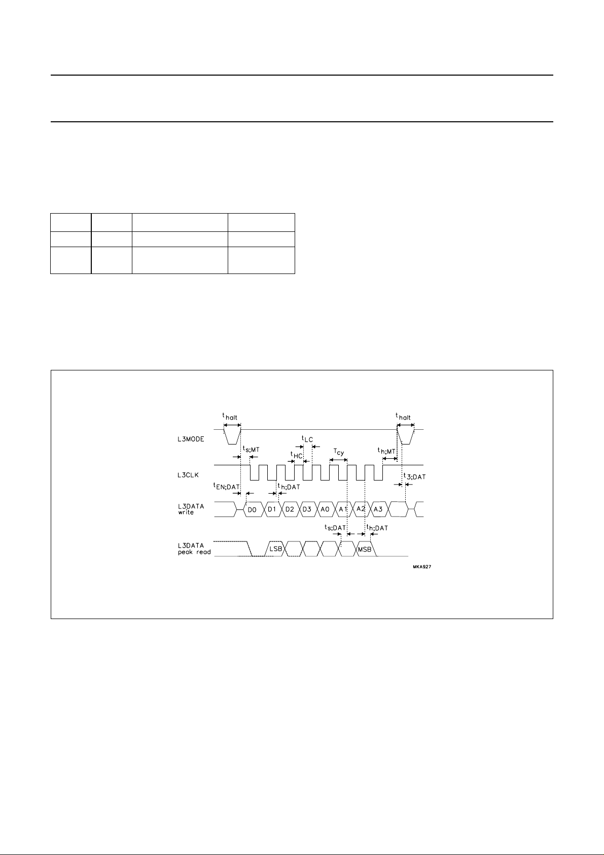
7.3.2 D
The selection performed in the address mode remains
active during subsequent data transfers, until the
TDA1546T receives a new address command. The
fundamental timing of data transfers is shown in Fig.7,
where L3DATA denotes the data from the TDA1546T to
the microcontroller (L3DATA write). The timing for the
opposite direction is essentially the same as in the address
mode (L3DATA read). The maximum input clock and data
rate is 64f
ATA TRANSFER MODE
(or 32fs when in the double-speed mode).
s
Fig.7 Timing for data transfer mode.
All transfers are bytewise, i.e. they are based on groups of
8 bits. Data will be stored in the TDA1546T after the eighth
bit of a byte has been received.
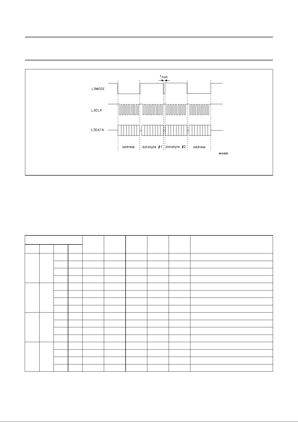
A multi-byte transfer is illustrated in Fig.8. The definition of
the L3 protocol allows for a so-called “halt” mode, as some
devices which are expected to connect to the same
microcontroller bus lines may require an indication of when
January 1995 11
8 bits have been transferred. This halt mode option is
implemented in the TDA1546T, meaning that subsequent
byte transfers must be separated by a period identified as
halt mode. A halt mode period is characterized by the
following conditions:
L3MODE = LOW, L3DATA = 3-state and L3CLK = HIGH.
Philips Semiconductors Preliminary specification
Bitstream Continuous Calibration DAC with
digital sound processing (BCC-DAC)
Fig.8 Multibyte transfer.
7.3.3 ORGANIZATION AND PROGRAMMING OF THE
INTERNAL REGISTER FILE
Command data received from the microcontroller is stored
in an internal register file (see Table 3) which is organized
as a page of 16 registers, each containing a 4-bit
command data word (D3 to D0).
TDA1546T
Access to the words in the register file involves selection
of the address of a register location (by means of A3, A2,
A1 and A0). A second page of 4 registers is accessible by
means of the extended address register bits (EA2, EA1
and EA0) and extended data register bits (ED3, ED2, ED1
and ED0).
Table 3 Microcontroller control register file
ADDRESS
D3 D2 D1 D0
A3 A2 A1 A0
0 0 0 0 BAL3 BAL2 BAL1 BAL0 1 1 1 1 balance left
0 1 BAR3 BAR2 BAR1 BAR0 1 1 1 1 balance right
1 0 VC3 VC2 VC1 VC0 1 1 1 1 volume control
1 1 VC7 VC6 VC5 VC4 1 1 1 0 volume control
0 1 0 0 FT3 FT2 FT1 FT0 0 0 0 0 fade time
0 1 DSS FP2 FP1 FP0 0 0 0 0 digital speaker system; 3 × band-pass
1 0 OVER3 OVER2 OVER1 OVER0 1 1 1 1 overload
1 1 SIL3 SIL2 SIL1 SIL0 0 0 0 0 silence level
1 0 0 0 SILT3 SILT2 SILT1 SILT0 0 0 0 0 silence time
0 1 MUTE OUTS1 OUTS0 SPOS 0 0 0 0 mute; 2 × output scaling; peak source
1 0 SCT3 SCT2 SCT1 SCT0 0 1 1 1 treble
1 1 SCB3 SCB2 SCB1 SCB0 0 1 1 0 bass
1 1 0 0 SCBB3 SCBB2 SCBB1 SCBB0 0 0 0 0 bass boost
0 1 FSO1 FSO0 DEMC1 DEMC0 0 0 0 0 2 × reserved; 2 × de-emphasis
1 0 ED3 ED2 ED1 ED0 1 1 1 1 extended data
1 1 RUNFA EA2 EA1 EA0 1 1 1 1 run fade; extended address
INITIAL
STATE
USED FOR
January 1995 12
 Loading...