

Philips TDA1543 Datasheet

INTEGRATED CIRCUITS
DATA SH EET
TDA1543
Dual 16-bit DAC (economy version)
2
(I
S input format)
Product specification
File under Integrated Circuits, IC01
February 1991
Philips Semiconductors Product specification
Dual 16-bit DAC (economy version)
2
(I
S input format)
FEATURES
• Low distortion
• 16-bit dynamic range
• 4 × oversampling possible
• Single 5 V power supply
• No external components required
• No requirement for external deglitcher circuitry due to
fast settling output current
• Adjustable bias current
• Internal timing and control circuits
• I2S input format: time multiplexed, two's complement,
TTL.
ORDERING INFORMATION
EXTENDED
TYPE NUMBER
TDA1543
TDA1543T
(1)
(2)
PINS PIN POSITION MATERIAL CODE
8 DIL plastic SOT97
16 mini-pack plastic SO16L;SOT162A
TDA1543
GENERAL DESCRIPTION
The TDA1543 is a monolithic integrated dual 16-bit
digital-to-analog converter (DAC) designed as an
economy version for use in hi-fi digital audio equipment
such as Compact Disc players, digital tape or cassette
recorders, digital sound in TV sets and in digital amplifiers.
PACKAGE
Notes
1. SOT97-1; 1996 August 13.
2. SOT162-1 1996 August 13.
QUICK REFERENCE DATA
SYMBOL PARAMETER CONDITIONS MIN. TYP. MAX. UNIT
V
DD
I
DD
I
FS
supply voltage 3.0 5.0 8.0 V
supply current − 50 60 mA
full scale output current 1.95 2.30 2.65 mA
THD total harmonic distortion including noise −−75 −70 dB
at 0 dB − 0.018 0.032 %
THD total harmonic distortion including noise −−30 −23 dB
at −60 dB − 3.2 7.9 %
t
cs
current settling time to ± 1 LSB − 0.5 −µs
BR input bit rate at data input −− 9.2 Mbits/s
f
BCK
clock frequency at clock input −− 9.2 MHz
S/N signal-to-noise ratio at bipolar zero 90 96 − dB
TC
FS
full scale temperature coefficient at analog outputs
−±500 × 10
−6
− K
−1
(AOL; AOR)
T
amb
operating ambient temperature
−30 −+85 °C
range
P
I
tot
bias
total power dissipation − 250 − mW
bias current (adjustable) −0.6 − 5.0 mA
February 1991 2
Philips Semiconductors Product specification
Dual 16-bit DAC (economy version)
2
(I
S input format)
3.3 nF
out
left
V
(2)
1.2 kΩ
AOL
6
BL
I
3.3 nF
1.2 kΩ
ref
V
AOL
I
out
right
V
(2)
ref
V
AOR
8
AOR
BR
I
I
5-BIT
DIVIDER
PASSIVE
TDA1543
5 V
bias
(1)
R
ref
V
7
ref
I
BR
I
BL
I
SOURCE
REFERENCE
TDA1543
nF
100
DD
V
5
ground
4
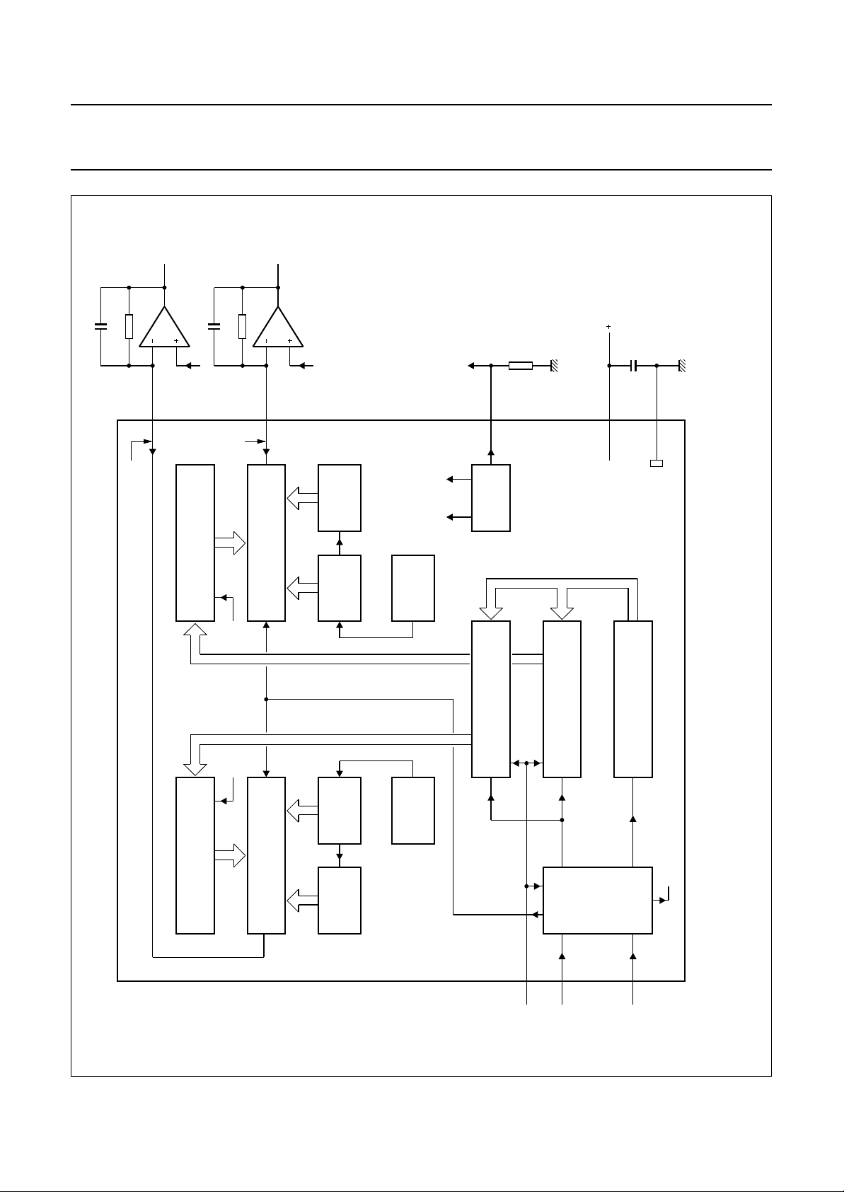
MEA110
RIGHT OUTPUT LATCH
LEFT OUTPUT LATCH
RIGHT BIT SWITCHES
LELE
LEFT BIT SWITCHES
11-BIT
PASSIVE
11-BIT
PASSIVE
5-BIT
PASSIVE
DIVIDER
DIVIDER
DIVIDER
SOURCE
CURRENT
SOURCE
CURRENT
LEFT INPUT LATCH
handbook, full pagewidth
Fig.1 Block diagram.
RIGHT INPUT LATCH
CONTROL
1
2
ADDRESS POINTER
LE
&
TIMING
3
February 1991 3
BCK
WS
DATA
(1) Optional.
(2) 2 × 1/2 NE5532.
Philips Semiconductors Product specification
Dual 16-bit DAC (economy version)
2
(I
S input format)
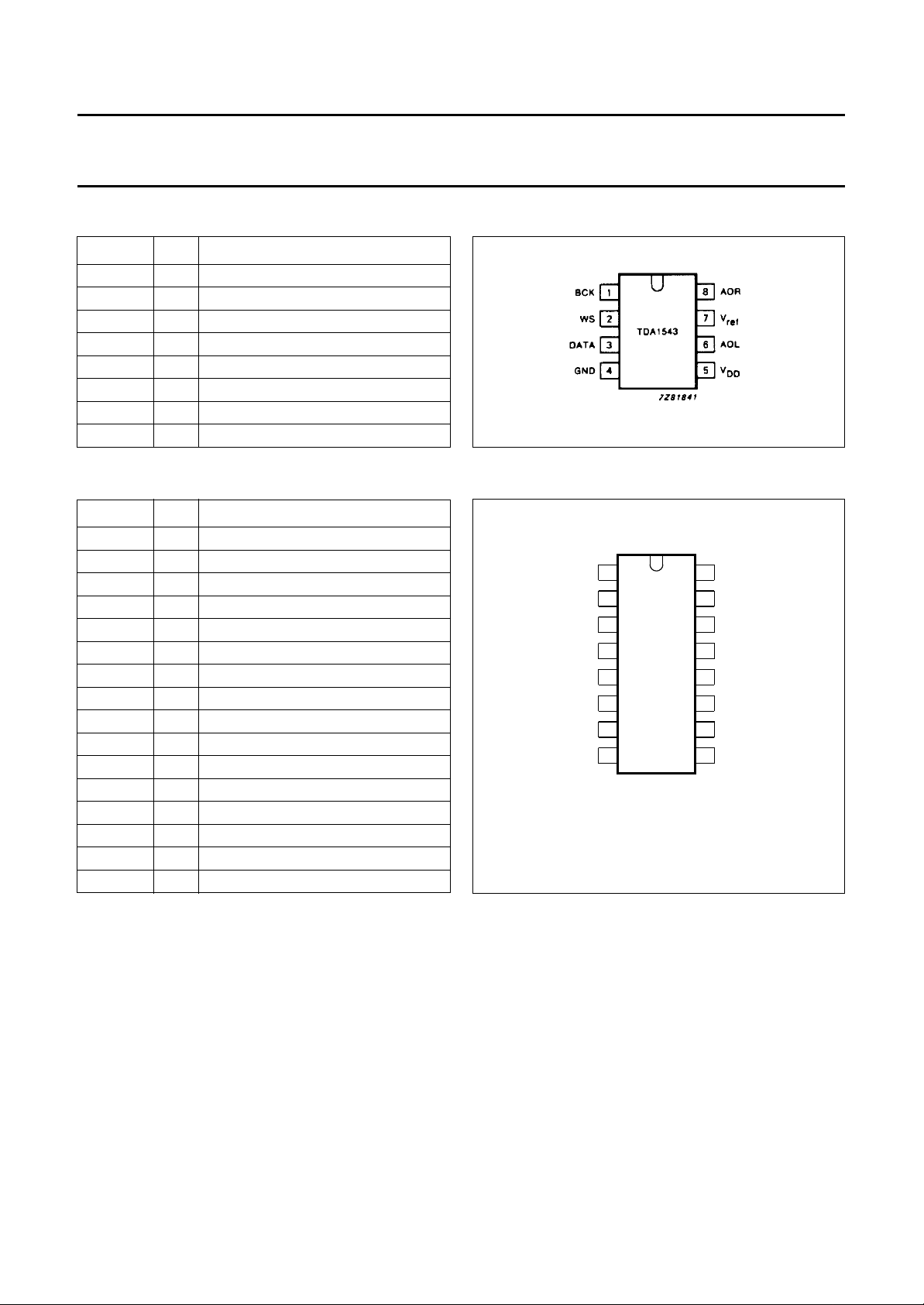
PINNING
SYMBOL PIN DESCRIPTION
BCK 1 bit clock input
WS 2 word select input
DATA 3 data input
GND 4 ground
V
DD
AOL 6 left channel voltage output
V
ref
AOR 8 right channel output
PINNING
SYMBOL PIN
n.c. 1 not connected
n.c. 2 not connected
BCK 3 bit clock input
WS 4 word select input
DATA 5 data input
GND 6 ground
n.c. 7 not connected
n.c. 8 not connected
n.c. 9 not connected
n.c. 10 not connected
V
DD
AOL 12 left channel output
V
ref
AOR 14 right channel output
n.c. 15 not connected
n.c. 16 not connected
5 +5 V supply voltage
7 reference voltage output
DESCRIPTION
11 +5 V supply voltage
13 reference voltage output
handbook, halfpage
Fig.3 Pin configuration TDA1543T.
TDA1543
Fig.2 Pin configuration TDA1543.
1
n.c.
2
n.c.
3
BCK AOR
4
WS
DATA
GND
n.c.
n.c.
TDA1543T
5
6
7
8
MEA107
16
n.c.
15
n.c.
14
V
13
ref
12
AOL
11
V
DD
10
n.c.
9
n.c.
February 1991 4
 Loading...