

Philips TDA1541A Datasheet

INTEGRATED CIRCUITS
DATA SH EET
TDA1541A
Stereo high performance 16-bit
DAC
Product specification
File under Integrated Circuits, IC01
February 1991
Philips Semiconductors Product specification
Stereo high performance 16-bit DAC TDA1541A
FEATURES
• High sound quality
• High performance: low noise and distortion, wide
dynamic range
• 4 × or 8 × oversampling possible
• Selectable two-channel input format
GENERAL DESCRIPTION
The TDA1541A is a stereo 16-bit digital-to-analog
converter (DAC). The ingenious design of the electronic
circuit guarantees a high performance and superior sound
quality. The TDA1541A is therefore extremely suitable for
use in top-end hi-fi digital audio equipment such as high
quality Compact Disc players or digital amplifiers.
• TTL compatible inputs.
ORDERING INFORMATION
EXTENDED TYPE
NUMBER
TDA1541A
(1)
PINS PIN POSITION MATERIAL CODE
28 DIL plastic SOT117
PACKAGE
Note
1. SOT117; SOT117-1; 1996 August 09.
QUICK REFERENCE DATA
SYMBOL PARAMETER CONDITIONS MIN. TYP. MAX. UNIT
V
−V
−V
I
DD
−I
−I
DD
DD1
DD2
DD1
DD2
supply voltage; pin 28 4.5 5.0 5.5 V
supply voltage; pin 26 4.5 5.0 5.5 V
supply voltage; pin 15 14.0 15.0 16.0 V
supply current; pin 28 − 27 40 mA
supply current; pin 26 − 37 50 mA
supply current; pin 15 − 25 35 mA
THD total harmonic distortion including noise −−95 −90 dB
at 0 dB − 0.0018 0.0032 %
THD total harmonic distortion including noise −−42 − dB
at −60 dB − 0.79 − %
NL non-linearity at T
t
cs
current settling time to ± 1LSB − 0.5 −µs
BR input bit rate at data input;
(pin 3 and 4)
f
BCK
TC
T
P
FS
amb
tot
clock frequency at clock input −−6.4 MHz
full scale temperature coefficient at analog
operating ambient temperature range −40 − +85 °C
total power dissipation − 700 − mW
=
amb
−20 to +85 °C
(AOL;AOR)
− 0.5 1.0 LSB
−−6.4 Mbits/s
−
±200 ×
-6
10
− K
-1
February 1991 2
Philips Semiconductors Product specification
Stereo high performance 16-bit DAC TDA1541A
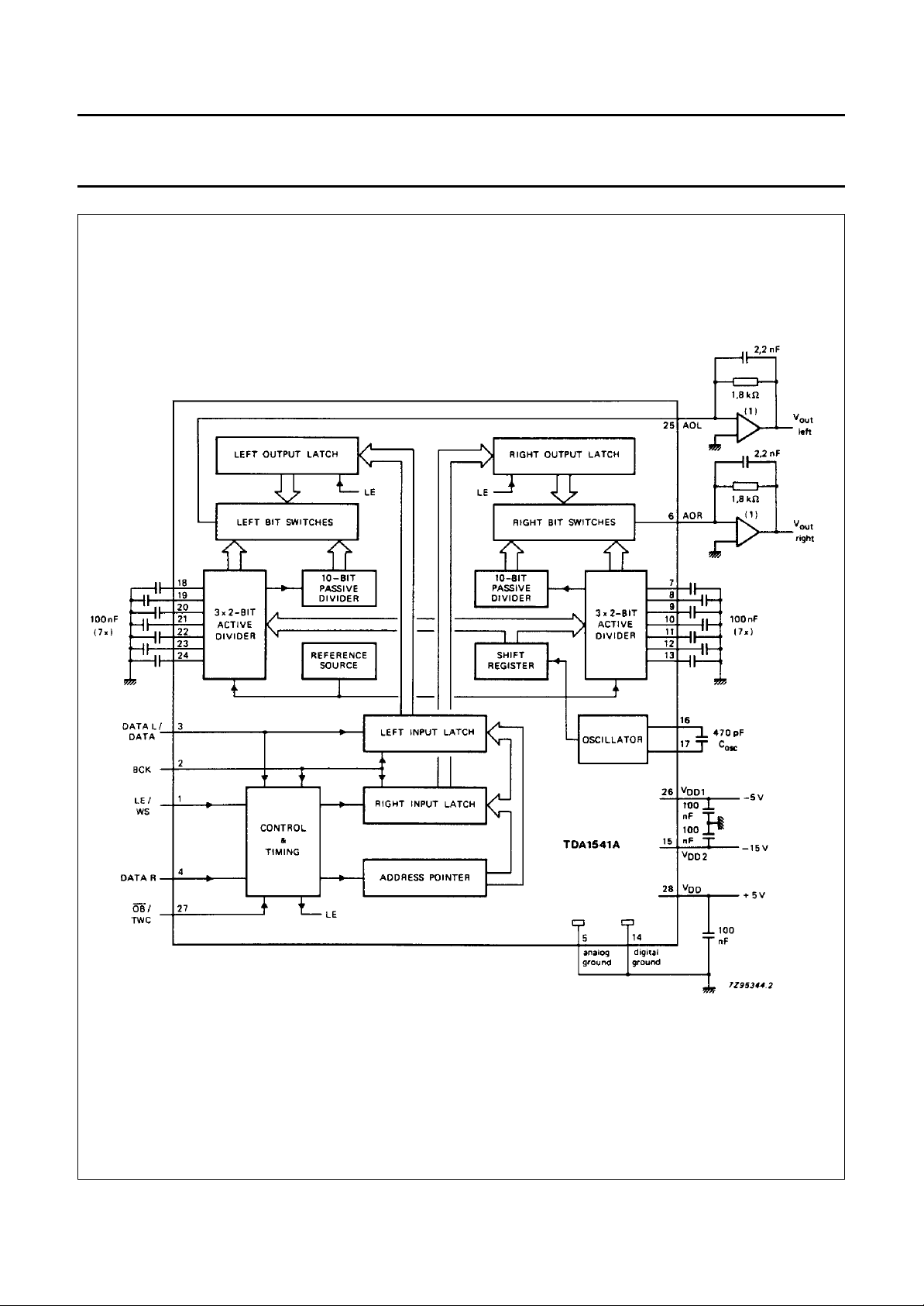
(1) TDA1542.
(2) 2 × NE5534 or equivalent.
Fig.1 Block diagram.
February 1991 3
Philips Semiconductors Product specification
Stereo high performance 16-bit DAC TDA1541A
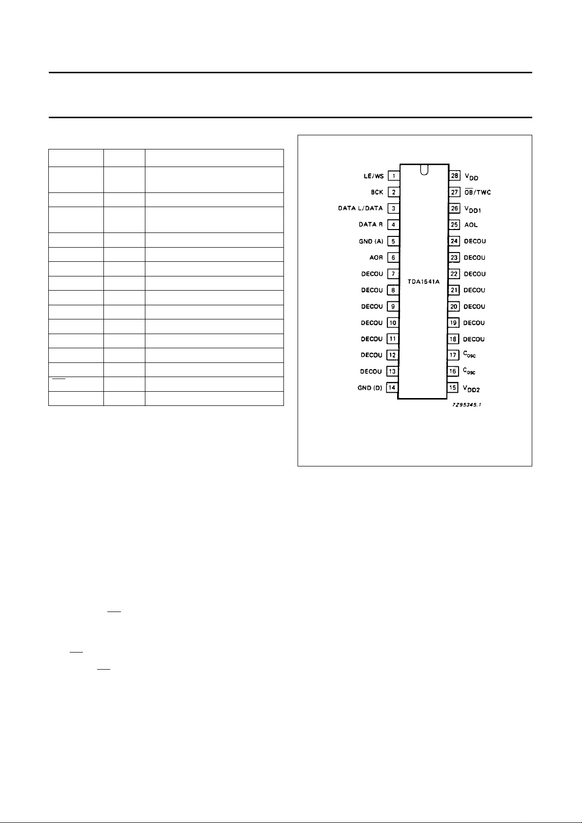
PINNING
SYMBOL PIN DESCRIPTION
(1)
LE/WS
(1)
BCK
DATA L
(1)
/DATA
DATA R
(1)
GND(A) 5 analog ground
AOR 6 right channel output
DECOU 7 to 13 decoupling
GND (D) 14 digital ground
V
DD2
15 −15 V supply voltage
COSC 16,17 oscillator
DECOU 18 to 24 decoupling
AOL 25 left channel output
V
DD1
OB/TWC
V
DD
(1)
26 −5 V supply voltage
27 mode select input
28 +5 V supply voltage
latch enable input/ word select
1
input
2 bit clock input
data left channel input/ data
3
input (selected format)
4 data right channel input
Note
1. See Table 1 data selection input.
Fig.2 Pin configuration
FUNCTIONAL DESCRIPTION
The TDA1541A accepts input sample formats in time multiplexed mode or simultaneous mode up to 16-bit word length.
The most significant bit (MSB) must always be first. The flexible input data format allows easy interfacing with signal
processing chips such as interpolation filters, error correction circuits, pulse code modulation adaptors and audio signal
processors (ASP).
The high maximum input bit-rate and fast setting facilitates application in 8 × oversampling systems
(44.1 kHz to 352.8 kHz or 48 kHz to 384 kHz) with the associated simple analog filtering function (low order, linear phase
filter).
Input data selection (see also Table 1)
With the input
OB/TWC connected to ground, data input (offset binary format) must be in time multiplexed mode. It is
accompanied with a word select (WS) and a bit clock input (BCK) signal. The converted samples appear at the output,
at the first positive going transition of the bit clock signal after a negative going transition of the word select signal.
With OB/TWC connected to VDD the mode is the same but the data format must be in the two’s complement.
When input OB/TWC input is connected to V
the two channels of data (L/R) are input simultaneously via DATA L and
DD1
DATA R, accompanied with BCK and a latch-enable input (LE). With this mode selected the data must be in offset binary.
The converted samples appear at the output at the positive going transition of the latch enable signal.
The format of the data input signals is shown in Fig.5 and 6.
February 1991 4
 Loading...