

Philips TDA1523 Datasheet

INTEGRATED CIRCUITS
DATA SH EET
TDA1523
Stereo cassette head
preamplifier and equalizer
Preliminary specification
File under Integrated Circuits, IC01
1996 Feb 26
Philips Semiconductors Preliminary specification
Stereo cassette head
preamplifier and equalizer
FEATURES
• Two independent amplifiers with open-loop gain of
90 dB (typical)
• Internal DC feedback via 140 kΩ resistor from output to
feedback point
• AC characteristics that can be determined externally by
an RC network
• Electronic on/off switching with transient suppression for
switch on
• Head input at DC ground that eliminates the input
coupling capacitor
• Minimum external component requirement
• Stability down to a gain of 30 dB
• Low input noise
• Low distortion
• DC input current <2 µA.
TDA1523
GENERAL DESCRIPTION
The TDA1523 is a playback amplifier for car radio/cassette
players.
QUICK REFERENCE DATA
SYMBOL PARAMETER CONDITIONS MIN. TYP. MAX. UNIT
V
P
I
P
T
amb
THD total harmonic distortion − 0.05 − %
α
cs
ORDERING INFORMATION
TYPE
NUMBER
TDA1523 DIP14 plastic dual in-line package; 14 leads (300 mil) SOT27-1
supply voltage (pin 7) 7.5 − 12 V
supply current (pin 7) − 5 − mA
operating ambient temperature −30 − +85 °C
channel separation RS=10kΩ; LS=0 45 −−dB
PACKAGE
NAME DESCRIPTION VERSION
1996 Feb 26 2
Philips Semiconductors Preliminary specification
Stereo cassette head
preamplifier and equalizer
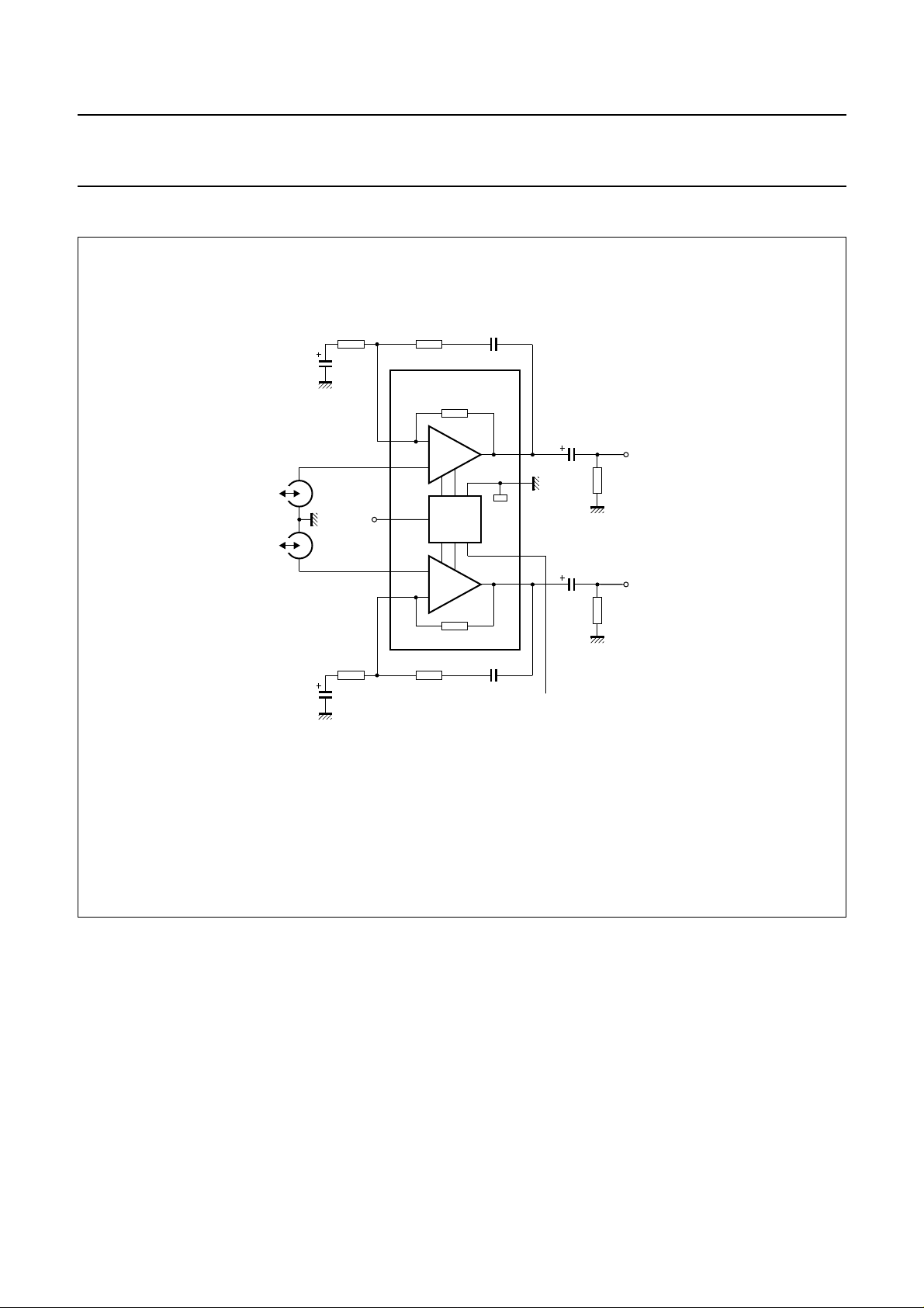
BLOCK DIAGRAM
handbook, full pagewidth
C102
220
µF
V
i1
V
i2
C202
220
µF
R102
8.2 Ω
R = 300 Ω
S1
L = 80 mH
S1
MUTE
R = 300 Ω
S2
L = 80 mH
S2
8.2 Ω
R101
5.6 kΩ
feedback 1
2
3
1
5
6
feedback 2
R201R202
5.6 kΩ
TDA1523
140 kΩ
R
fb1
AMP 1
SUPPLY
&
MUTE
AMP 2
R
fb2
140 kΩ
C101
22 nF
C201
22 nF
TDA1523
C
c1
14
4
7
8
output 1
10 µF
C
c2
output 2
10 µF
V
P
MGC988
R
L1
4.7 kΩ
R
L2
4.7 kΩ
V
o1
V
o2
Fig.1 Block diagram with external components; also used as test circuit.
1996 Feb 26 3

Philips Semiconductors Preliminary specification
Stereo cassette head
preamplifier and equalizer
PINNING
SYMBOL PIN DESCRIPTION
MUTE 1 mute input
FB1 2 feedback 1
V
i1
GND 4 ground
V
i2
FB2 6 feedback 2
V
P
V
o2
n.c. 9 not connected
n.c. 10 not connected
n.c. 11 not connected
n.c. 12 not connected
n.c. 13 not connected
V
o1
3 input voltage 1
5 input voltage 2
7 power supply
8 output voltage 2
14 output voltage 1
handbook, halfpage
1
MUTE
2
FB1
3
V
i1
4
GND
V
FB2
V
TDA1523
5
i2
6
7
P
MGC989
Fig.2 Pin configuration.
TDA1523
14
V
o1
13
n.c.
12
n.c.
11
n.c.
10
n.c.
9
n.c.
8
V
o2
1996 Feb 26 4
Philips Semiconductors Preliminary specification
Stereo cassette head
TDA1523
preamplifier and equalizer
LIMITING VALUES
In accordance with the Absolute Maximum Rating System (IEC 134); note 1.
SYMBOL PARAMETER MIN. MAX. UNIT
V
P
I
fb
P
tot
T
amb
T
stg
Note
1. All pins except 2 and 6 (feedback) can be connected to VP (pin 7) or ground (pin 4).
CHARACTERISTICS
V
= 8.5 V; T
P
SYMBOL PARAMETER CONDITIONS MIN. TYP. MAX. UNIT
Supply (pin 7)
V
P
I
P
Inputs (pins 3 or 5)
V
ni(rms)
V
ni
I
ni
, I
I
3
5
Z
input impedance f = 1 kHz; note 1 200 −−kΩ
i
Outputs (pins 14 or 8); see Fig.7
V
o
I
O
V
O
V
no(rms)
V
no
V
no
Z
output impedance f = 1 kHz; note 1 −−1kΩ
o
supply voltage (pin 7) 7.5 12 V
feedback current (pins 2 and 6) − 10 mA
total power dissipation − 300 mW
operating ambient temperature −30 +85 °C
storage temperature −55 +150 °C
=25°C; see test circuit Fig.1; unless otherwise specified.
amb
supply voltage 7.5 − 12 V
supply current − 5 − mA
unweighted noise input voltage
(RMS value)
noise input voltage RS= 0; f = 1 kHz; measured
f = 20 Hz to 20 kHz;
measured in Fig.3
− 1.6 −
− 5 −
in Fig.3; see also Fig.5
noise input current f = 1 kHz; measured in Fig.3;
− 1.2 −
see also Fig.6
DC input current at pins 3 and 5 −−−2µA
output voltage Vi= 0.3 mV; f = 315 Hz − 0.72 − V
THD = 1%; f = 1 kHz 1.0 −−V
output source current V
≥ 7.5 V; mute off −5 −10 − mA
1-4
DC output voltage − 3.7 − V
weighted noise output voltage;
RS= 300 Ω; LS=80mH − 700 −µV
DIN A (RMS value)
weighted noise output voltage
CCITT (peak value) R
CCIR (peak value) R
unweighted noise output voltage;
= 300 Ω; LS=80mH − 1200 −µV
S
= 300 Ω; LS=80mH − 1600 −µV
S
RS= 300 Ω; LS=80mH − 1800 −µV
DIN 45405 (peak value)
µV
nV
----------- Hz
pA
----------- Hz
1996 Feb 26 5
 Loading...