

Philips TDA1521Q-N5, TDA1521-N5, TDA1521-N4 Datasheet

DATA SH EET
Product specification
File under Integrated Circuits, IC01
July 1994
INTEGRATED CIRCUITS
TDA1521
TDA1521Q
2 x 12 W hi-fi audio power amplifier

July 1994 2
Philips Semiconductors Product specification
2 x 12 W hi-fi audio power amplifier
TDA1521
TDA1521Q
GENERAL DESCRIPTION
The TDA1521/TDA1521Q is a dual hi-fi audio power amplifier encapsulated in a 9-lead plastic power package.
The device is especially designed for mains fed applications (e.g. stereo tv sound and stereo radio).
Features
• Requires very few external components
• Input muted during power-on and off
(no switch-on or switch-off clicks)
• Low offset voltage between output and ground
• Excellent gain balance between channels
• Hi-fi according to IEC 268 and DIN 45500
• Short-circuit-proof
• Thermally protected
QUICK REFERENCE DATA
PACKAGE OUTLINES
TDA1521: 9 leads in-line; plastic power (SOT131); SOT131-1; 1996 August 20.
TDA1521Q: 9 leads SIL-bent-to-DIL; plastic power (SOT157); SOT157-2; 1996 August 20.
Stereo applications
Supply voltage range V
P
± 7,5 to ± 21,0 V
Output power at THD = 0,5%,
V
P
= ± 16 V P
O
typ. 12 W
Voltage gain G
v
typ. 30 dB
Gain balance between channels ∆G
v
typ. 0,2 dB
Ripple rejection SVRR typ. 60 dB
Channel separation α typ. 70 dB
Noise output voltage V
no(rms)
typ. 70 µV
July 1994 3
Philips Semiconductors Product specification
2 x 12 W hi-fi audio power amplifier
TDA1521
TDA1521Q
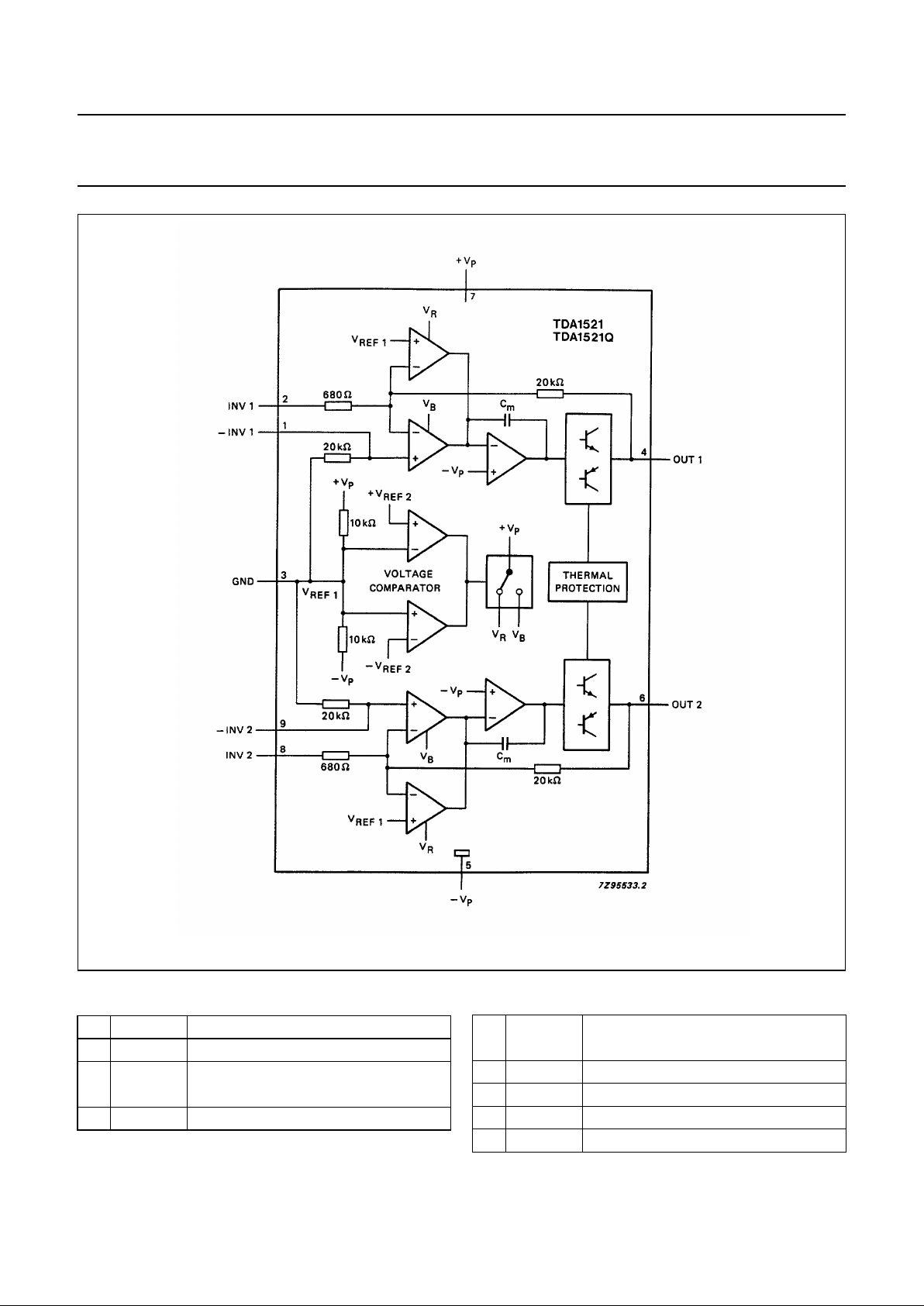
Fig.1 Block diagram.
PINNING
1 −INV1 non-inverting input 1
2 INV1 inverting input 1
3 GND
ground (symmetrical)
1
⁄2 VP (asymmetrical)
4 OUT1 output 1
5 −V
P
negative supply (symmetrical)
ground (asymmetrical)
6 OUT2 output 2
7+V
P
positive supply
8 INV2 inverting input 2
9 −INV2 non-inverting input 2

July 1994 4
Philips Semiconductors Product specification
2 x 12 W hi-fi audio power amplifier
TDA1521
TDA1521Q
FUNCTIONAL DESCRIPTION
This hi-fi stereo power amplifier is designed for mains fed applications. The circuit is designed for both symmetrical and
asymmetrical power supply systems. An output power of 2 × 12 watts (THD = 0,5%) can be delivered into an 8 Ω load
with a symmetrical power supply of ± 16 V.
The gain is fixed internally at 30 dB. Internal gain fixing gives low gain spread and very good balance between the
amplifiers (0,2 dB).
A special feature of this device is a mute circuit which suppresses unwanted input signals during switching on and off.
Referring to Fig.13, the 100 µF capacitor creates a time delay when the voltage at pin 3 is lower than an internally fixed
reference voltage. During the delay the amplifiers remain in their DC operating mode but are isolated from the
non-inverting inputs on pins 1 and 9.
Two thermal protection circuits are provided, one monitors the average junction temperature and the other the
instantaneous temperature of the power transistors. Both protection circuits activate at 150 °C allowing safe operation to
a maximum junction temperature of 150°C without added distortion.
RATINGS
Limiting values in accordance with the Absolute Maximum System (IEC 134)
Note
For asymmetrical power supplies (at short circuiting of the load) the maximum supply voltage is limited to VP = 28 V.
If the total internal resistance of the supply (Ri) > 4 Ω, the maximum unloaded supply voltage is increased to 32 V.
PARAMETER CONDITIONS SYMBOL MIN. MAX. UNIT
Supply voltage pin 7 V
P
= V
7-3
− +21 V
pin 5 −V
P
= V
5-3
−−21 V
Non-repetitive peak
output current pins 4 and 6 I
OSM
− 4A
Total power dissipation see Fig.2 P
tot
Storage temperature range T
stg
−55 +150 °C
Junction temperature T
j
− 150 °C
Short-circuit time: see note
outputs short-circuited
to ground symmetrical
(full signal drive) power supply t
sc
− 1 hour
asymmetrical
power supply;
V
P
< 32 V
(unloaded);
R
i
≥ 4 Ω t
sc
− 1 hour
July 1994 5
Philips Semiconductors Product specification
2 x 12 W hi-fi audio power amplifier
TDA1521
TDA1521Q
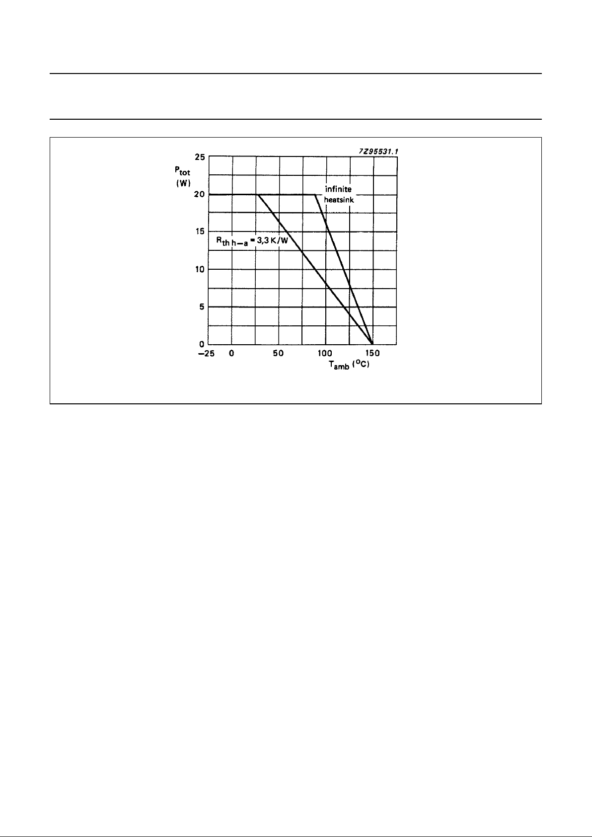
Fig.2 Power derating curve.
THERMAL RESISTANCE
HEATSINK DESIGN EXAMPLE
With derating of 2,5 K/W, the value of heatsink thermal resistance is calculated as follows:
given RL = 8 Ω and VP = ±16 V, the measured maximum dissipation is 14,6 W; then, for a maximum ambient temperature
of 65 °C, the required thermal resistance of the heatsink is
Note: The internal metal block (heatsink) has the same potential as pin 5 (−V
P
).
From junction to case R
th j-c
= 2,5 K/W
R
th h a–
150 65–
14 6,
----------------------
25 33 K W⁄,=,–=
 Loading...