

Philips TDA1521Q, TDA1521 Datasheet

INTEGRATED CIRCUITS
DATA SH EET
TDA1521
TDA1521Q
2 x 12 W hi-fi audio power amplifier
Product specification
File under Integrated Circuits, IC01
July 1994

Philips Semiconductors Product specification
2 x 12 W hi-fi audio power amplifier
TDA1521
TDA1521Q
GENERAL DESCRIPTION
The TDA1521/TDA1521Q is a dual hi-fi audio power amplifier encapsulated in a 9-lead plastic power package.
The device is especially designed for mains fed applications (e.g. stereo tv sound and stereo radio).
Features
• Requires very few external components
• Input muted during power-on and off
(no switch-on or switch-off clicks)
• Low offset voltage between output and ground
• Excellent gain balance between channels
• Hi-fi according to IEC 268 and DIN 45500
• Short-circuit-proof
• Thermally protected
QUICK REFERENCE DATA
Stereo applications
Supply voltage range V
Output power at THD = 0,5%,
V
= ± 16 V P
P
Voltage gain G
Gain balance between channels ∆G
Ripple rejection SVRR typ. 60 dB
Channel separation α typ. 70 dB
Noise output voltage V
P
O
v
no(rms)
± 7,5 to ± 21,0 V
typ. 12 W
typ. 30 dB
typ. 0,2 dB
v
typ. 70 µV
PACKAGE OUTLINES
TDA1521: 9 leads in-line; plastic power (SOT131); SOT131-1; 1996 August 20.
TDA1521Q: 9 leads SIL-bent-to-DIL; plastic power (SOT157); SOT157-2; 1996 August 20.
July 1994 2
Philips Semiconductors Product specification
2 x 12 W hi-fi audio power amplifier
TDA1521
TDA1521Q
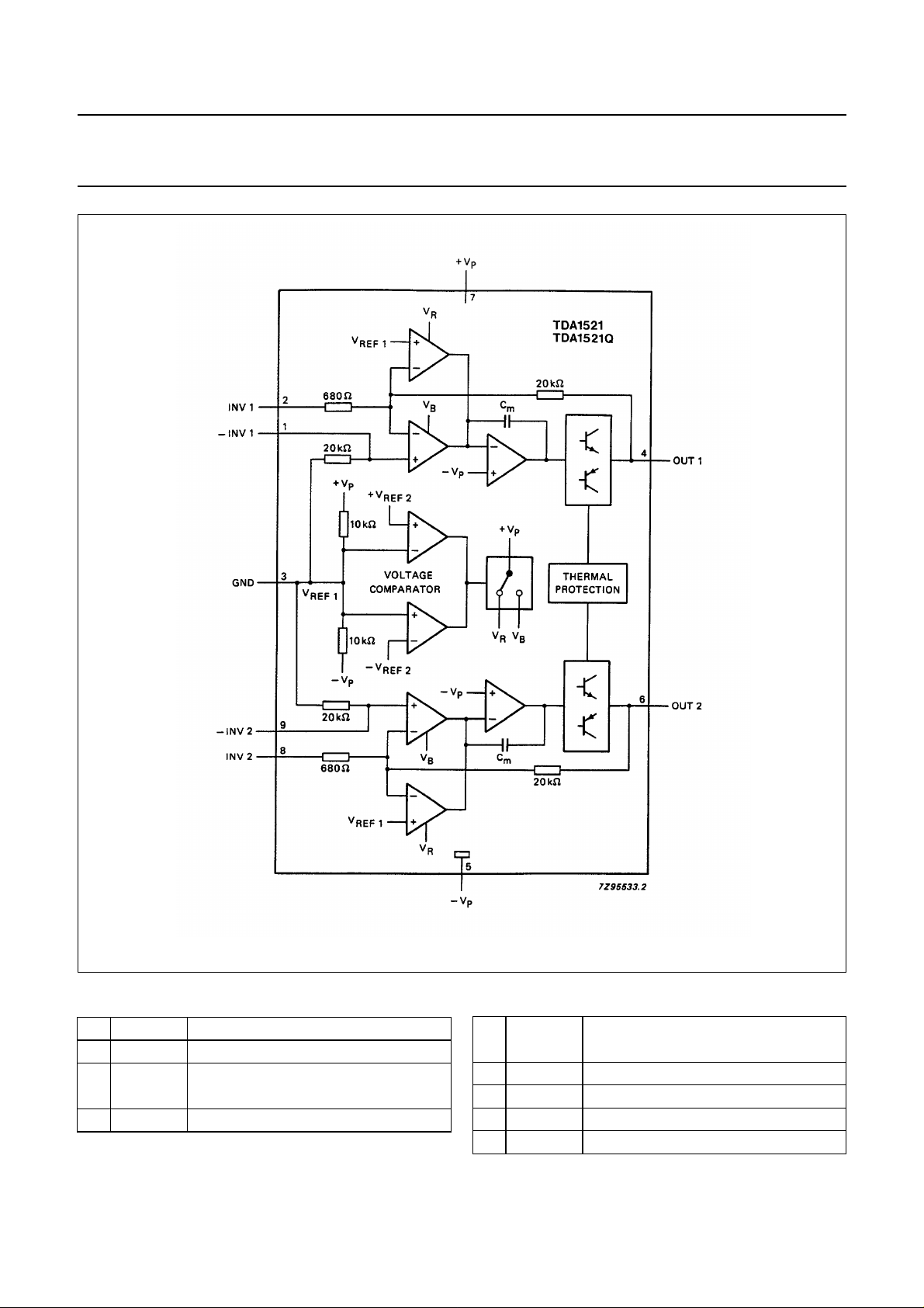
Fig.1 Block diagram.
PINNING
1 −INV1 non-inverting input 1
2 INV1 inverting input 1
3 GND
4 OUT1 output 1
July 1994 3
ground (symmetrical)
1
⁄2 VP (asymmetrical)
5 −V
6 OUT2 output 2
7+V
8 INV2 inverting input 2
9 −INV2 non-inverting input 2
P
P
negative supply (symmetrical)
ground (asymmetrical)
positive supply

Philips Semiconductors Product specification
2 x 12 W hi-fi audio power amplifier
TDA1521
TDA1521Q
FUNCTIONAL DESCRIPTION
This hi-fi stereo power amplifier is designed for mains fed applications. The circuit is designed for both symmetrical and
asymmetrical power supply systems. An output power of 2 × 12 watts (THD = 0,5%) can be delivered into an 8 Ω load
with a symmetrical power supply of ± 16 V.
The gain is fixed internally at 30 dB. Internal gain fixing gives low gain spread and very good balance between the
amplifiers (0,2 dB).
A special feature of this device is a mute circuit which suppresses unwanted input signals during switching on and off.
Referring to Fig.13, the 100 µF capacitor creates a time delay when the voltage at pin 3 is lower than an internally fixed
reference voltage. During the delay the amplifiers remain in their DC operating mode but are isolated from the
non-inverting inputs on pins 1 and 9.
Two thermal protection circuits are provided, one monitors the average junction temperature and the other the
instantaneous temperature of the power transistors. Both protection circuits activate at 150 °C allowing safe operation to
a maximum junction temperature of 150°C without added distortion.
RATINGS
Limiting values in accordance with the Absolute Maximum System (IEC 134)
PARAMETER CONDITIONS SYMBOL MIN. MAX. UNIT
Supply voltage pin 7 V
pin 5 −V
Non-repetitive peak
output current pins 4 and 6 I
Total power dissipation see Fig.2 P
Storage temperature range T
Junction temperature T
Short-circuit time: see note
outputs short-circuited
to ground symmetrical
(full signal drive) power supply t
asymmetrical
power supply;
< 32 V
V
P
(unloaded);
R
≥ 4 Ω t
i
P
OSM
tot
stg
j
sc
sc
= V
= V
P
7-3
5-3
− +21 V
−−21 V
− 4A
−55 +150 °C
− 150 °C
− 1 hour
− 1 hour
Note
For asymmetrical power supplies (at short circuiting of the load) the maximum supply voltage is limited to VP = 28 V.
If the total internal resistance of the supply (Ri) > 4 Ω, the maximum unloaded supply voltage is increased to 32 V.
July 1994 4
Philips Semiconductors Product specification
2 x 12 W hi-fi audio power amplifier
TDA1521
TDA1521Q
Fig.2 Power derating curve.
THERMAL RESISTANCE
From junction to case R
HEATSINK DESIGN EXAMPLE
With derating of 2,5 K/W, the value of heatsink thermal resistance is calculated as follows:
given RL = 8 Ω and VP = ±16 V, the measured maximum dissipation is 14,6 W; then, for a maximum ambient temperature
of 65 °C, the required thermal resistance of the heatsink is
R
th h a–
Note: The internal metal block (heatsink) has the same potential as pin 5 (−V
150 65–
---------------------14 6,
25 33 K W⁄,=,–=
th j-c
= 2,5 K/W
).
P
July 1994 5
 Loading...