

Philips TDA1519CTH, TDA1519CSP Datasheet

INTEGRATED CIRCUITS
DATA SH EET
TDA1519C
22 W BTL or 2 × 11 W
stereo power amplifier
Product specification
Supersedes data of 2000 Mar 08
File under Integrated Circuits, IC01
2001 Aug 24

Philips Semiconductors Product specification
22 W BTL or 2 × 11 W
stereo power amplifier
FEATURES
• Requires very fewexternal components for Bridge-Tied
Load (BTL) operation
• Stereo or BTL application
• High output power
• Low offset voltage at output (important for BTL
applications)
• Fixed gain
• Good ripple rejection
• Mute/standby switch
• Load dump protection
• AC and DC short-circuit safe to ground and V
• Thermally protected
• Reverse polarity safe
• Capability to handle high energy on outputs (VP=0V)
• No switch-on/switch-off plops
• Protected against electrostatic discharge
• Low thermal resistance
• Identical inputs (inverting and non-inverting)
• Pin compatible with TDA1519B (TDA1519C and
TDA1519CSP).
P
TDA1519C
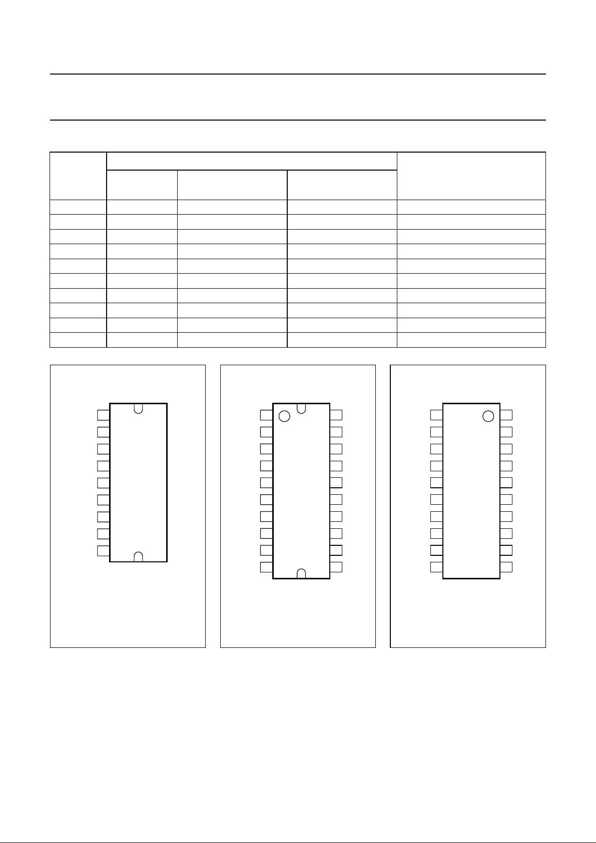
GENERAL DESCRIPTION
The TDA1519C is an integrated class-B dual output
amplifierin a 9-leadplastic single in-linepower package or
20-lead heatsink small outline package.
For the TDA1519CTH (SOT418-2), the heatsink is
positioned on top of the package,which allows anexternal
heatsink to be mounted on top. The heatsink of the
TDA1519CTD (SOT397-1) is facing the PCB, allowing the
heatsink to be soldered onto the copper area of the PCB.
ORDERING INFORMATION
TYPE NUMBER
NAME DESCRIPTION VERSION
TDA1519C SIL9P plastic single in-line power package; 9 leads SOT131-2
TDA1519CSP SMS9P plastic surface mounted single in-line power package; 9 leads SOT354-1
TDA1519CTD HSOP20 plastic, heatsink small outline package; 20 leads SOT397-1
TDA1519CTH HSOP20 plastic, heatsink small outline package; 20 leads; low stand-off height SOT418-2
PACKAGE
2001 Aug 24 2

Philips Semiconductors Product specification
22 W BTL or 2 × 11 W
TDA1519C
stereo power amplifier
QUICK REFERENCE DATA
SYMBOL PARAMETER CONDITIONS MIN. TYP. MAX. UNIT
Supply
V
P
I
ORM
I
q(tot)
I
stb
I
sw(on)
Inputs
input impedance BTL 25 −−kΩ
Z
i
Stereo application
P
o
α
cs
V
n(o)(rms)
BTL application
P
o
SVRR supply voltage ripple rejection R
∆V
DC output offset voltage −−250 mV
OO
T
j
supply voltage operating 6.0 14.4 17.5 V
non-operating −−30 V
load dump protected −−45 V
repetitive peak output current −−4A
total quiescent current − 40 80 mA
standby current − 0.1 100 µA
switch-on current −−40 µA
stereo 50 −−kΩ
output power THD = 10%
=4Ω−6−W
R
L
R
=2Ω−11 − W
L
channel separation 40 −−dB
noise output voltage (RMS value) − 150 −µV
output power THD = 10%; RL=4Ω−22 − W
=0Ω
S
f
= 100 Hz 34 −−dB
i
f
= 1 to 10 kHz 48 −−dB
i
junction temperature −−150 °C
2001 Aug 24 3

Philips Semiconductors Product specification
22 W BTL or 2 × 11 W
stereo power amplifier
BLOCK DIAGRAM
handbook, full pagewidth
NINV
RR
TDA1519C
switch
VA
15 kΩ
15 kΩ
mute switch
VA
18.1 kΩ
V
P
18.1 kΩ
C
m
+
+
−
mute
reference
voltage
power stage
+
−
TDA1519C
TDA1519CSP
standby
reference
voltage
mute
switch
4
OUT1
8
M/SS
1
60
kΩ
183
Ω
standby
× 1
3
power stage
183
Ω
9
INV
60
kΩ
input
reference
voltage
GND1 GND2V
The pin numbers refer to the TDA1519C and TDA1519CSP only, for TDA1519CTD and TDA1519CTH see Figs 3 and 4.
VA
C
m
mute switch
signal
ground
2 7
power
ground
(substrate)
5
P
6
MGL491
Fig.1 Block diagram.
2001 Aug 24 4
OUT2
Philips Semiconductors Product specification
22 W BTL or 2 × 11 W
TDA1519C
stereo power amplifier
PINNING
PIN
SYMBOL
TDA1519C;
TDA1519CSP
TDA1519CTD TDA1519CTH
NINV 1 19 19 non-inverting input
GND1 2 20 20 ground 1 (signal)
RR 3 1 1 supply voltage ripple rejection
OUT1 4 3 3 output 1
GND2 5 5 5 ground 2 (substrate)
OUT2 6 8 8 output 2
V
P
7 10 10 positive supply voltage
M/SS 8 11 11 mute/standby switch input
INV 9 12 12 inverting input
n.c. − 2, 4, 6, 7, 9 and 13 to 18 2, 4, 6, 7, 9 and 13 to 18 not connected
DESCRIPTION
alfpage
NINV
GND1
RR
OUT1
GND2
OUT2
V
M/SS
INV
1
2
3
4
5
6
7
P
8
9
TDA1519C
TDA1519CSP
Fig.2 Pin configuration
TDA1519C and
TDA1519CSP.
MGR561
page
RR
n.c.
OUT1
n.c.
GND2
n.c.
n.c.
OUT2
n.c.
V
1
2
3
4
5
6
7
8
9
10
P
TDA1519CTD
Fig.3 Pin configuration
TDA1519CTD.
MGL937
GND1
20
19
NINV
18
n.c.
17
n.c.
16
n.c.
15
n.c.
n.c.
14
n.c.
13
INV
12
M/SS
11
page
GND1
NINV
n.c.
n.c.
n.c.
n.c.
n.c.
n.c.
INV
M/SS
20
19
18
17
16
TDA1519CTH
15
14
13
12
11
MGL936
RR
1
n.c.
2
OUT1
3
n.c.
4
GND2
5
n.c.
6
n.c.
7
8
OUT2
n.c.
9
V
10
P
Fig.4 Pin configuration
TDA1519CTH.
2001 Aug 24 5
Philips Semiconductors Product specification
22 W BTL or 2 × 11 W
TDA1519C
stereo power amplifier
FUNCTIONAL DESCRIPTION
The TDA1519C contains two identical amplifiers with
differential input stages. The gain of each amplifier isfixed
at 40 dB. A special feature of this device is the
mute/standby switch which has the following features:
LIMITING VALUES
In accordance with the Absolute Maximum Rating System (IEC 60134).
SYMBOL PARAMETER CONDITIONS MIN. MAX. UNIT
V
P
V
sc
V
rp
E
o
I
OSM
I
ORM
P
tot
T
j
T
stg
supply voltage operating − 17.5 V
AC and DC short-circuit-safe voltage − 17.5 V
reverse polarity voltage − 6V
energy handling capability at outputs VP=0V − 200 mJ
non-repetitive peak output current − 6A
repetitive peak output current − 4A
total power dissipation see Fig.5 − 25 W
junction temperature − 150 °C
storage temperature −55 +150 °C
• Low standby current (<100 µA)
• Low mute/standby switching current (allows for low-cost
supply switch)
• Mute condition.
non-operating − 30 V
load dump protected;
− 45 V
during 50 ms; tr≥ 2.5 ms
(1) Infinite heatsink.
(2) R
(3) R
th(c-a)
th(c-a)
= 5 K/W.
= 13 K/W.
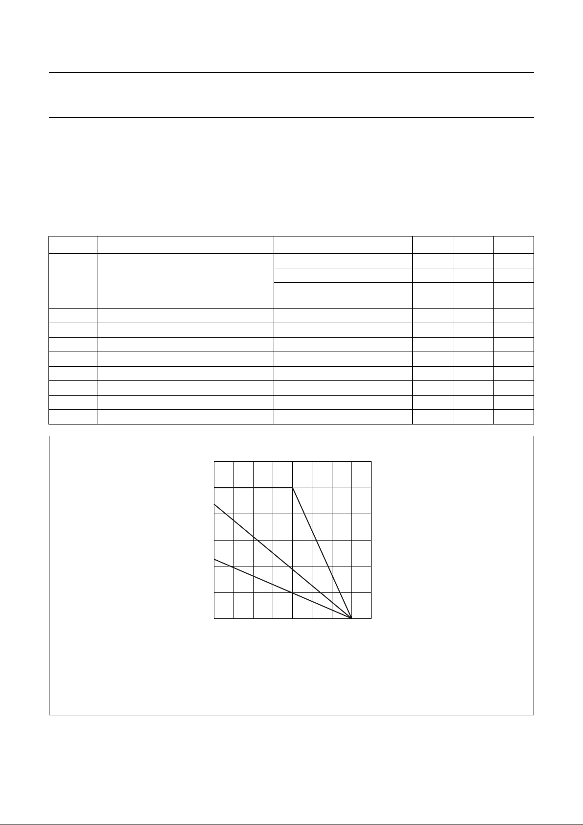
30
handbook, halfpage
P
tot
(W)
20
10
0
−25 0 50 150
(1)
(2)
(3)
100
T
Fig.5 Power derating curve for TDA1519C.
amb
MGL492
(°C)
2001 Aug 24 6
 Loading...