

Philips TDA1519A Technical data

查询TDA1519A供应商
INTEGRATED CIRCUITS
DATA SH EET
TDA1519A
22 W BTL or 2 x 11 W stereo car
radio power amplifier
Product specification
File under Integrated Circuits, IC01
May 1992

Philips Semiconductors Product specification
22 W BTL or 2 x 11 W stereo car radio
TDA1519A
power amplifier
GENERAL DESCRIPTION
The TDA1519A is an integrated class-B dual output amplifier in a 9-lead single in-line (SIL) plastic power package.
The device is primarily developed for car radio applications.
Features
• Requires very few external components for Bridge Tied
Load (BTL)
• Stereo or BTL application
• High output power
• Low offset voltage at output (important for BTL)
• Fixed gain
• Good ripple rejection
• Mute/stand-by switch
• Load dump protection
• AC and DC short-circuit-safe to ground and V
P
QUICK REFERENCE DATA
• Thermally protected
• Reverse polarity safe
• Capability to handle high energy on outputs (VP= 0 V)
• No switch-on/switch-off plop
• Protected against electrostatic discharge
• Low thermal resistance
• Identical inputs (inverting and non-inverting)
• Compatible with TDA1519B (except output power).
PARAMETER CONDITIONS SYMBOL MIN. TYP. MAX. UNIT
Supply voltage range
operating V
non-operating V
load dump protected V
Repetitive peak output current I
Total quiescent current I
Stand-by current I
Switch-on current I
P
P
P
ORM
tot
sb
sw
6.0 14.4 17.5 V
−−30 V
−−45 V
−−4A
− 40 80 mA
− 0.1 100 µA
−−40 µA
Input impedance
BTL |ZI|25−−kΩ
stereo |Z
|50−−kΩ
I
Stereo application
Output power THD = 10%; 4 Ω P
THD = 10%; 2 Ω P
o
o
− 6 − W
− 11 − W
Channel separation α 40 −−dB
Noise output voltage V
no(rms)
− 150 −µV
May 1992 2

Philips Semiconductors Product specification
22 W BTL or 2 x 11 W stereo car radio
power amplifier
PARAMETER CONDITIONS SYMBOL MIN. TYP. MAX. UNIT
BTL application
Output power THD = 10%; 4 Ω P
Supply voltage ripple rejection R
DC output offset voltage |∆V
Crystal temperature T
PACKAGE OUTLINES
9 lead SIL; plastic power (SOT131); SOT131-2; 1996 July 22.
9-lead SIL-bent-to-DIL; plastic power (SOT157); SOT157-2; 1996 July 22.
= 0 Ω
S
f = 100 Hz RR 34 −−dB
f = 1 kHz to 10 kHz RR 48 −−dB
o
| −−250 mV
0
c
TDA1519A
− 22 − W
−−150 °C
May 1992 3
Philips Semiconductors Product specification
22 W BTL or 2 x 11 W stereo car radio
power amplifier
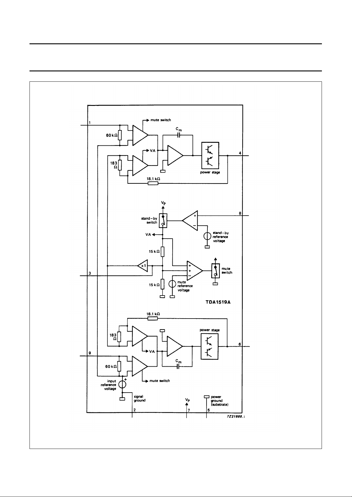
TDA1519A
Fig.1 Block diagram.
May 1992 4

Philips Semiconductors Product specification
22 W BTL or 2 x 11 W stereo car radio
TDA1519A
power amplifier
PINNING
1 NINV non-inverting input
2 GND1 ground (signal)
3 RR supply voltage ripple rejection
4 OUT1 output 1
5 GND2 ground (substrate)
6 OUT2 output 2
7V
P
8 M/SS mute/stand-by switch
9 INV inverting input
FUNCTIONAL DESCRIPTION
The TDA1519A contains two identical amplifiers with differential input stages. The gain of each amplifier is fixed at 40 dB.
A special feature of this device is the mute/stand-by switch which has the following features:
• Low stand-by current (< 100 µA)
• Low mute/stand-by switching current (low cost supply switch)
• Mute condition.
positive supply voltage
RATINGS
Limiting values in accordance with the Absolute Maximum System (IEC 134)
PARAMETER CONDITIONS SYMBOL MIN. MAX. UNIT
Supply voltage
operating V
non-operating V
load dump protected during 50 ms;
t
≥ 2.5 ms
r
AC and DC short-circuit-safe voltage V
Reverse polarity V
Energy handling capability at outputs V
= 0 V − 200 mJ
P
Non-repetitive peak output current I
Repetitive peak output current I
Total power dissipation see Fig.2 P
Crystal temperature T
Storage temperature range T
P
P
V
P
PSC
PR
OSM
ORM
tot
c
stg
− 17.5 V
− 30 V
− 45 V
− 18 V
− 6V
− 6A
− 4A
− 25 W
− 150 °C
−55 + 150 °C
May 1992 5
 Loading...