

Philips tda1518b DATASHEETS

INTEGRATED CIRCUITS
DATA SH EET
TDA1518BQ
24 W BTL or 2 x 12 watt stereo
car radio power amplifier
Product specification
File under Integrated Circuits, IC01
July 1994

Philips Semiconductors Product specification
24 W BTL or 2 x 12 watt stereo
TDA1518BQ
car radio power amplifier
GENERAL DESCRIPTION
The TDA1518BQ is an integrated class-B output amplifier in a 13-lead single-in-line (SIL) plastic power package.
The device is primarily developed for car radio applications.
FEATURES
• Requires very few external components
• Flexibility in use stereo as well as mono BTL
• High output power (without bootstrap)
• Low offset voltage at output (important for BTL)
• Fixed gain
• Good ripple rejection
• Mute/stand-by switch
• Load dump protection
• A.C. and d.c. short-circuit-safe to ground and V
QUICK REFERENCE DATA
PARAMETER CONDITIONS SYMBOL MIN. TYP. MAX. UNIT
P
• Thermally protected
• Reverse polarity safe
• Capability to handle high energy on outputs (VP= 0 V)
• No switch-on/switch-off plop
• Flexible leads
• Low thermal resistance
• Identical inputs (inverting and non-inverting)
• Compatible with TDA1516BQ (except gain).
Supply voltage range
operating V
non-operating V
load dump V
P
P
P
6,0 14,4 18,0 V
−−30,0 V
−−45,0 V
Repetitive peak output
current I
Total quiescent current I
Stand-by current l
Switch-on current I
ORM
tot
sb
sw
−−4A
− 30 − mA
− 0,1 100 µA
−−40 µA
Input impedance
BTL |Z
stereo |Z
|25−−kΩ
I
|50−−kΩ
I
Stereo application
Output power THD = 10%; 4 Ω P
THD = 10%; 2 Ω P
o
o
− 6 − W
− 11 − W
Channel separation α 40 −−dB
Noise output voltage V
no(rms)
− 150 −µV
BTL application
Output power THD = 10%, 4 Ω P
Supply voltage R
ripple rejection f = 100 Hz to 10 kHz RR 48 −−dB
D.C. output offset voltage |∆V
July 1994 2
= 0 Ω;
S
o
| −−250 mV
O
− 22 − W
Philips Semiconductors Product specification
24 W BTL or 2 x 12 watt stereo
car radio power amplifier
PACKAGE OUTLINE
13-lead SIL-bent-to-DIL; plastic power (SOT141C); SOT141-6; 1996 July 19.
TDA1518BQ
July 1994 3
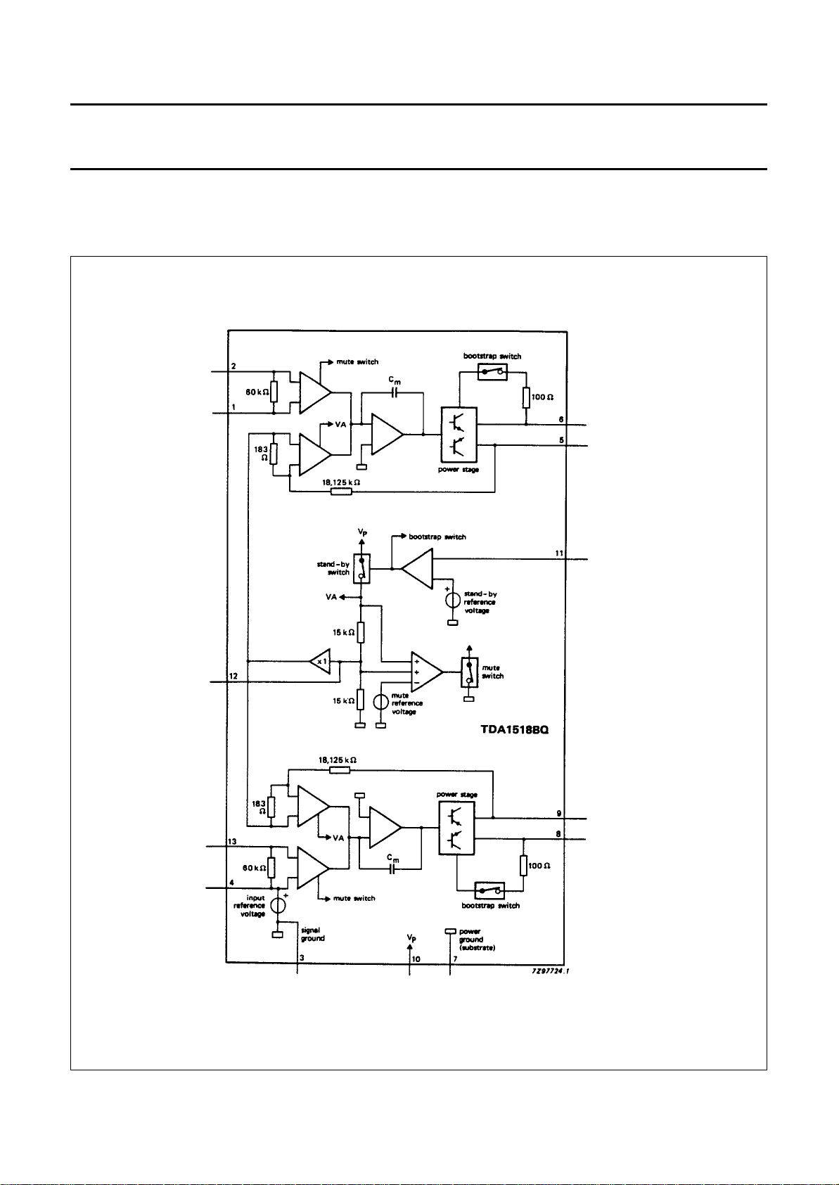
Fig.1 Block diagram.

Philips Semiconductors Product specification
24 W BTL or 2 x 12 watt stereo
TDA1518BQ
car radio power amplifier
PINNING
1 −INV1 non-inverting input 1 8 BS2 bootstrap 2
2 INV inverting input 9 OUT2 output 2
3 GND1 ground (signal) 10 V
4V
ref
reference voltage 11 M/SS mute/stand-by switch
P
5 OUT1 output 1 12 RR supply voltage ripple rejection
6 BS1 bootstrap 1 13 −INV2 non-inverting input 2
7 GND2 ground (substrate)
FUNCTIONAL DESCRIPTION
The TDA1518BQ contains two identical amplifiers with differential input stages. This device can be used for stereo or
bridge applications. The gain of each amplifier is fixed at 40 dB. A special feature of this device is the mute/stand-by
switch which has the following features:
• low stand-by current (< 100 µA)
• low mute/stand-by switching current (low cost supply switch)
• mute condition.
supply voltage
RATINGS
Limiting values in accordance with the Absolute Maximum System (IEC 134)
PARAMETER CONDITIONS SYMBOL MIN. MAX. UNIT
Supply voltage
operating V
non-operating V
P
P
− 18 V
− 30 V
load dump during 50 ms;
≥ 2,5 ms V
t
r
P
− 45 V
A.C. and d.c. short-circuit-
safe voltage V
Reverse polarity V
PSC
PR
− 18 V
− 6V
Energy handling capability
at outputs VP= 0 V − 200 mJ
Non-repetitive peak output
current I
OSM
− 6A
Repetitive peak output
current I
Total power dissipation see Fig.2 P
Crystal temperature T
Storage temperature range T
ORM
tot
c
stg
− 4A
− 25 W
− 150 °C
−55 +150 °C
July 1994 4
 Loading...