

Page 1

INTEGRATED CIRCUITS
DATA SH EET
TDA10045H
DVB-T channel receiver
Product specification
Supersedes data of 2000 Jun 21
File under Integrated Circuits, IC02
2001 Nov 08
Page 2

Philips Semiconductors Product specification
DVB-T channel receiver TDA10045H
FEATURES
• 2 and 8 kbytes Coded Orthogonal Frequency Division
Multiplexer (COFDM) demodulator (fully DVB-T
compliant: ETSI 300-744)
• All modes supported, including hierarchical modes
• Fully automatic transmission parameters detection
(including Fast Fourier Transformer (FFT) size and
guard interval)
• Digital Signal Processor (DSP) based synchronization
(software can be upgraded on the fly)
• No extra-host software required
• On-chip 10-bit Analog-to-Digital Converter (ADC)
• 2nd or 1st IF variable analog input
• Only fundamental crystal oscillator required (4 MHz
typical ±100 ppm)
• 6, 7 and 8 MHz channels with the same crystal
• Pulse killer algorithm to protect against impulse noise
• Digital frequency correction (±90 kHz)
• Frequency offset (±1/6MHz) automatic estimator to
speed-up the scan
• RF tuner input power measurement
• Parallel or serial transport stream interface
• BER measurement (before and after Viterbi decoder)
• Signal-to noise ratio estimation
• Constellation, CSI and channel frequency response
outputs
• TPS bits I2C-bus readable (including spare ones)
• Controllable dedicated I2C-bus for the tuner
(5 V tolerant)
• 3 low frequency spare DACs and 2 spare inputs
• CMOS 0.2 µm technology.
GENERAL DESCRIPTION
The TDA10045H is a single-chip channel receiver for
2 and 8 kbytes COFDM modulated signals based on the
ETSI specification (ETSI 300-744). The device interfaces
directly to anIF signal, which could be either 1st or 2nd IF
and integrates a 10-bit Analog-to-Digital Converter (ADC),
a Numerically Controlled Oscillator (NCO) and a
Phase-Locked Loop (PLL), simplifying external logic
requirements and limiting system costs.
The TDA10045H performs all the COFDM demodulation
tasks from IF signal to the MPEG-2 transport stream. An
internal DSP core manages the synchronization and the
control of the demodulation process, and implements
specially developed software for robustness against
co-channelandadjacent channel interference, to deal with
Single Frequency Network (SFN) echo situations, and to
assist in a very fast scan of the bandwidth. After baseband
conversion and FFT demodulation, the channel frequency
response is estimated, which is based on the scattered
pilots, and filtered in both time and frequency domains.
This estimation is used as a correction on the signal,
carrier by carrier. A common phase error and estimator is
usedtodealwiththetunerphasenoise.The Forward Error
Correction (FEC) decoder is automatically synchronized
by the frame synchronization algorithm that uses the TPS
information included in the modulation. An embedded
‘pulse killer’ algorithm enables the bad effects of short and
strong impulsive noise interference that could be caused
by electrical domestic devices and/or car traffic to be
greatly reduced.
APPLICATIONS
• DVB-T fully compatible
• Digital data transmission using COFDM modulation.
2001 Nov 08 2
This device is controlled via an I2C-bus (master). The chip
provides 2 switchable I2C-buses derived from the master:
a tuner I2C-bus to be disconnected from the I2C-bus
master when not necessary and an EEPROM I2C-bus.
The DSP software code can be fed to the chip via the
master I2C-bus or via the dedicated EEPROM I2C-bus.
Designed in 0.2 µm CMOS technology and housed in a
100 pin QFP package, the TDA10045H operates over the
commercial temperature range.
Page 3

Philips Semiconductors Product specification
DVB-T channel receiver TDA10045H
ORDERING INFORMATION
TYPE
NUMBER
TDA10045H QFP100 plastic quad flat package; 100 leads (lead length 1.95 mm);
NAME DESCRIPTION
body 14 × 20 × 2.8 mm
PACKAGE
VERSION
SOT317-2
2001 Nov 08 3
Page 4
This text is here in white to force landscape pages to be rotated correctly when browsing through the pdf in the Acrobat reader.This text is here in
_white to force landscape pages to be rotated correctly when browsing through the pdf in the Acrobat reader.This text is here inThis text is here in
white to force landscape pages to be rotated correctly when browsing through the pdf in the Acrobat reader. white to force landscape pages to be ...
2001 Nov 08 4
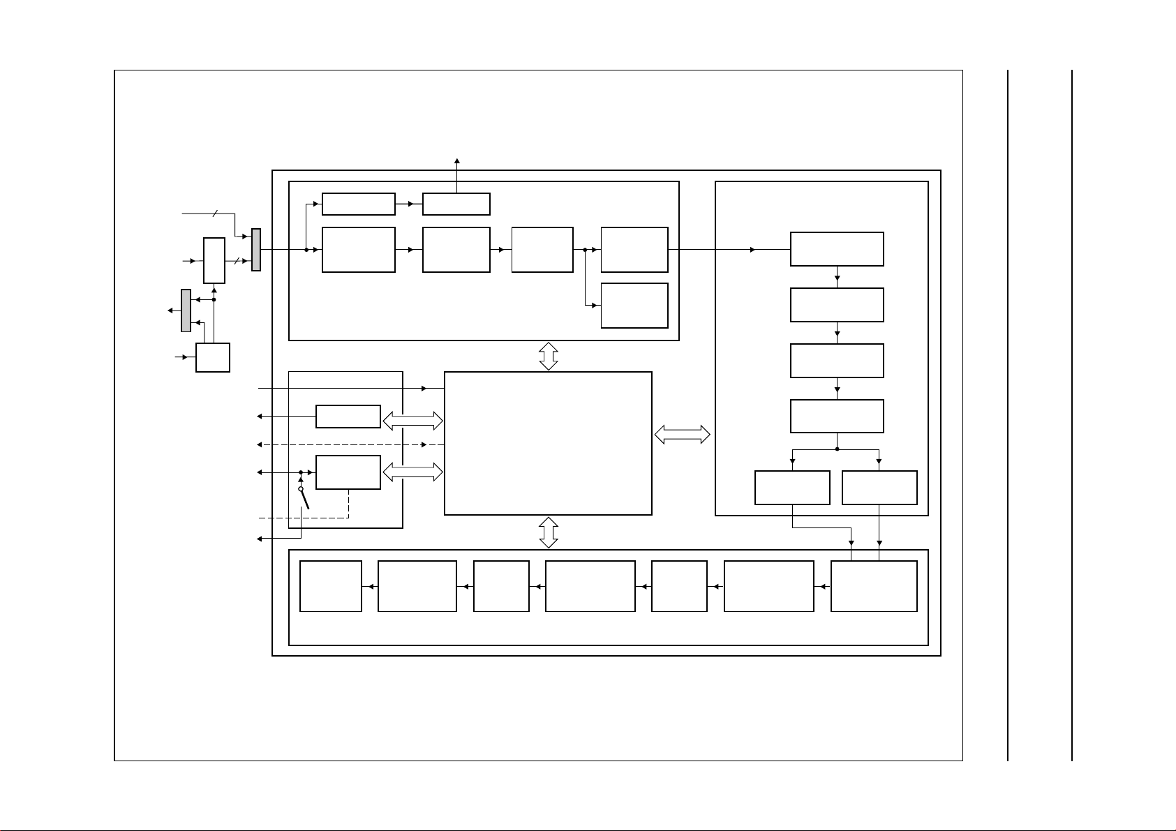
VAGC
BLOCK DIAGRAM
Philips Semiconductors Product specification
DVB-T channel receiver TDA10045H
digital IF
FI (9:0)
analog IF
(VIM, VIP)
SACLK
XIN
10
A
10
D
C
f
s
2f
s
PLL
SP_IN(1:0)
DS_SPARE(3:1)
SCL_EEP
SDA_EEP
SCL
SDA
SCL_TUN
SDA_TUN
BASEBAND
CONVERSION
spare inputs
3 SPARE ∆Σ
optional
I2C-BUS
INTERFACE
MPEG-2
OUTPUT
INTERFACE
RECOVERY
3* 10
DESCRAMBLER
CPT_UNCOR
DIGITAL FRONT-END
∆ΣAGC
TIME
(NCO)
CARRIER
RECOVERY
AND COFDM
DEMODULATION
DSP CORE
SYNCHRONIZATION
FREQUENCY, TIME, FRAME, RECOVERY
FFT WINDOW POSITIONING
TPS DECODING
RS
DECODER
CHANNEL DECODER
OUTER
FORNEY
DE-INTERLEAVER
FFT
COARSE
TIME
ESTIMATOR
TDA10045H
VBER
VITERBI
DECODER
COFDM
spectrum
CONFIDENCE
CALCULATION
confidence
frequency response
BIT
DE-INTERLEAVER
CBER
CHANNEL ESTIMATION
AND CORRECTION
CPE
CALCULATION
PARTIAL CHANNEL
ESTIMATION
TIME
INTERPOLATION
FREQUENCY
INTERPOLATION
CHANNEL
CORRECTION
(I,Q)
constellation
INNER
FREQUENCY
DE-INTERLEAVER
AND DE-MAPPER
Fig.1 Block diagram.
handbook, full pagewidth
MGU414
Page 5

Philips Semiconductors Product specification
DVB-T channel receiver TDA10045H
PINNING
SYMBOL PIN TYPE DESCRIPTION
V
DDD33
V
SSD
DS_SPARE3 3 O spare delta-sigma output; managed by the DSP to generate an analog level
VAGC 4 O output value from the Delta-Sigma modulator, used to control a log-scaled
SCL_EEP 5 O extra I
V
DDD33
V
SSD
SDA_EEP 8 I/OD extra I
SCL_TUN 9 OD
SDA_TUN 10 I/OD tuner I
SCL 11 I
SDA 12 I/OD I
n.c. 13 − not connected
CLR# 14 I
EEPADDR 15 I
SADDR[1:0] 16 and 17 I
V
DDD18
V
SSD
TM[3:0] 20 to 23 I
SCAN_EN 24 I
V
DDD50
V
SSD
DWNLOAD 27 I
SP_IN[1:0] 28 and 29 I
1 − digital supply voltage for the pads (3.3 V typ.)
2 − digital ground supply (0 V
(after a RC low-pass filter)
amplifier (after analog filtering)
2
C-bus clock to download DSP code from an external EEPROM (optional
mode); can be connected to the master I2C-bus
6 − digital supply voltage for the pads (3.3 V typ.)
7 − digital ground supply (0 V)
2
C-bus data bus to download DSP code from an external EEPROM
(optional mode). It can be connected to the master I2C-bus; this pin is
open-drain which requires an external pull-up resistor (to V
DDD33
or V
DDD50
even if not used.
(1)
tuner I2C-bus serial clock signal; this signal is derived from the master SCL and
is open-drain which requires an external pull-up resistor (to V
DDD33
or V
DDD50
even if not used
2
C-bus serial data signal; this signal is derived from the master SDA and
is open-drain which requires an external pull-up resistor (to V
DDD33
or V
DDD50
even if not used
(2)
I2C-bus master serial clock; up to 700 kbit/s
2
C-bus master serial data input/output, open-drain I/O pad, which requires an
external pull-up resistor (to V
(2)
asynchronous reset signal; active LOW
(2)
EEPADDR is the LSB of the I2C-bus address of the EEPROM. The MSBs are
DDD33
or V
DDD50
)
internally set to 101000. Therefore the complete I2C-bus address of the
EEPROM is (MSB to LSB): 1, 0, 1, 0, 0, 0, EEPADDR.
(2)
SADDR[1:0] are the 2 LSBs of the I2C-bus address of the TDA10045; the MSBs
are internally set to 00010; therefore the complete I2C-bus address of the
TDA10045 is (MSB to LSB): 0, 0, 0, 1, 0, SADDR[1] and SADDR[0]
18 − digital supply voltage for the core (1.8 V typ.)
19 − digital ground supply (0 V)
(2)
test mode bus; for test purpose; must be set to ‘0000’
(2)
scan enable for production test; connected to GND
25 − digital supply voltage (5 V typ.); can be set to 3.3 V (with caution) if the 5 V
tolerant I/O is not required
26 − digital ground supply (0 V)
(2)
processor control, boot mode; if set to logic 0, the DSP downloads the software
from an external EEPROM on the dedicated I2C-bus (pins SDA_EEP and
SCL_EEP). If set to logic 1 the software is downloaded in the I2C-bus register
CODE_IN from the host; in this case the external EEPROM is not needed.
(2)
spare inputs
),
),
),
2001 Nov 08 5
Page 6

Philips Semiconductors Product specification
DVB-T channel receiver TDA10045H
SYMBOL PIN TYPE DESCRIPTION
FFT_WIN 30 I/O output or input signal indicating the start of the active data; equals 1 during
complex sample 0 of the active FFT block; can be used to synchronize 2 chips
V
DDD33
V
SSD
SACLK 33 O sampling frequency output; this output clock can be fed to an external (10-bit)
FI[9:5] 34 to 38 I/O input data from an external ADC, FI must be tied to ground when unused,
V
DDD18
V
SSD
FI[4:0] 41 to 45 IO input data from an external ADC, FI must be tied to ground when unused,
V
DDD50
V
SSD
IT 48 OD
FEL 49 OD
n.c. 50 − not connected
n.c. 51 − not connected
TRSTN 52 I
TMS 53 I
TDI 54 I
TCK 55 I
TDO 56 O output port for boundary scan; not connected if not used
V
DDD18
V
SSD
DS_SPARE2 59 O spare delta-sigma output; managed by the DSP or by an I
DS_SPARE1 60 O spare delta-sigma output; managed by the DSP to handle a low frequency DAC
V
DDD33
V
SSD
UNCOR 63 O RS error flag, active HIGH on one RS packet if the RS decoder fails to correct
PSYNC 64 O pulse synchro; this output signal goes HIGH on a rising edge of OCLK when a
31 − digital supply voltage for the pads (3.3 V typ.)
32 − digital ground supply (0 V)
ADC as a sampling clock; SACLK can also provide twice the sampling clock
positive notation (from 0 to 1023) or twos complement notation (from
−512 to +511). In internal ADC mode, these outputs can be used to monitor
extra demodulator output signals (constellation or frequency response).
39 − digital supply voltage for the core (1.8 V typ.)
40 − digital ground supply (0 V)
positive notation (from 0 to 1023) or twos complement notation (from
−512 to +511). In internal ADC mode, these outputs can be used to monitor
extra demodulator output signals (constellation or frequency response).
46 − digital supply voltage (5 V typ.); can be set to 3.3 V (with caution) if 5 V tolerant
I/O is not required
47 − digital ground supply (0 V)
(1)
interrupt line; this output interrupt line can be configured by the I2C-bus
interface. This pin is an open-drain output and therefore requires an external
pull-up resistor (to V
(1)
front-end lock; FEL is an open-drain output and therefore requires an external
pull-up resistor (to V
(2)
asynchronous reset signal for boundary scan; connected to GND if not used
(2)
mode programming signal for boundary scan; connected to GND if not used
(2)
input port for boundary scan; connected to GND if not used
(2)
clock signal for boundary scan; connected to GND if not used)
DDD33
DDD33
or V
or V
DDD50
DDD50
).
)
57 − digital supply voltage for the core (1.8 V typ.)
58 − digital ground supply (0 V)
2
C-bus register to
generate an analog level (after a RC low-pass filter)
(automatic first stage tuner AGC measurement or 2nd AGC loop control as
examples)
61 − digital supply voltage for the pads (3.3 V typ.)
62 − digital ground supply (0 V)
the errors
synchro byte is provided, then goes LOW until the next synchro byte
2001 Nov 08 6
Page 7

Philips Semiconductors Product specification
DVB-T channel receiver TDA10045H
SYMBOL PIN TYPE DESCRIPTION
DEN 65 O outputdata validation signal; active HIGH during the valid and regular data bytes
OCLK 66 O output clock; OCLK is the output clock for the parallel DO[7:0] outputs
DO[7:5] 67 to 69 O output data carrying the current sample of the current MPEG2 packet
(188 bytes), delivered on the rising edge of OCLK by default when the serial
mode is selected. The output data is delivered by DO[0].
V
DDD18
V
SSD
DO[4:0] 72 to 76 O output data carrying the current sample of the current MPEG2 packet
V
DDD33
V
SSD
XIN 79 I
XOUT 80 O crystal oscillator output pin; typically a fundamental crystal oscillator is
V
DDD18
V
SSD
n.c. 83 − not connected
V
CCD(PLL)
DGND 85 − ground return for the digital circuits of the PLL module
n.c. 86 − not connected
PPLGND 87 − ground return for the analog circuits of the PLL module
V
CCA(PLL)
V
SSA3
V
DDA3
V
IP
V
IM
V
ref(neg)
V
ref(pos)
V
DDA3
V
SSA3
V
SSA2
V
DDA2
V
SSA1
V
DDD1
70 − digital supply voltage for the core (1.8 V typ.)
71 − digital ground supply (0 V)
(188 bytes), delivered on the rising edge of OCLK by default when the serial
mode is selected. The output data is delivered by DO[0].
77 − digital supply voltage for the pads (3.3 V typ.)
78 − digital ground supply (0 V)
(2)
crystal oscillator input pin
connected between pins XIN and XOUT
81 − digital supply voltage for the core (1.8 V typ.)
82 − digital ground supply (0 V)
84 − power supply input for the digital circuits of the PLL module (1.8 V typ.)
88 − power supply input for the analog circuits of the PLL module (3.3 V typ.)
89 − ground return for the analog circuits
90 − power supply input for the analog circuits; the DC voltage should be 3.3 V
91 − positive input to the ADC; this pin is DC biased to half supply through an internal
resistor divider (2 × 20 kΩ resistors). In order to remain in the range of the ADC,
the voltage difference between pins VIP and VIM should be between −0.5 and
+0.5 V.
92 − negative input to the ADC; this pin is DC biased to half supply to remain in the
range of the ADC, the voltage difference between pins VIP and VIM should be
between −0.5 and +0.5 V through an internal resistor divider (2 × 20 kΩ
resistors)
93 − negative reference voltage for the ADC
94 − positive reference voltage for the ADC
95 − power supply input for the analog circuits; the DC voltage should be 3.3 V
96 − ground return for analog circuits
97 − ground return for the analog clock drivers
98 − power supply input for the analog clock drivers; the DC voltage should be 3.3 V
99 − ground return for the digital switching circuitry
100 − power supply input for the digital switching circuitry; sensitive to the supply
noise; the DC voltage should be 1.8 V
2001 Nov 08 7
Page 8

Philips Semiconductors Product specification
DVB-T channel receiver TDA10045H
Notes
1. OD are open-drain outputs, so they must be connected to a pull-up resistor to either V
2. All inputs (I) are TTL, 5 V tolerant, (if V
is set to 5 V).
DD50
3. Foundry test I/O inputs must be connected to GND.
DDD33
or V
DDD50
handbook, full pagewidth
V
DDD33
V
SSD
DS_SPARE3
VAGC
SCL_EEP
V
DDD33
V
SSD
SDA_EEP
SCL_TUN
SDA_TUN
SCL
SDA
CLR#
EEPADDR
SADDR[1]
SADDR[0]
V
DDD18
V
SSD
TM[3]
TM[2]
TM[1]
TM[0]
SCAN_EN
V
DDD50
V
SSD
DWNLOAD
SP_IN[1]
SP_IN[0]
FFT_WIN
n.c.
DDD1VSSA1VDDA2VSSA2VSSA3VDDA3Vref(pos)Vref(neg)VIMVIPVDDA3VSSA3VCCA(PLL)
V
99989796959493929190898887868584838281
100
1
2
3
4
5
6
7
8
9
10
11
12
13
14
15
16
17
18
19
20
21
22
23
24
25
26
27
28
29
TDA10045H
PPLGND
n.c.
DGND
V
CCD(PLL)
SSDVDDD18
n.c.
V
XOUT
80
XIN
79
V
78
V
77
DO[0]
76
DO[1]
75
DO[2]
74
DO[3]
73
DO[4]
72
V
71
V
70
DO[5]
69
DO[6]
68
DO[7]
67
OCLK
66
DEN
65
PSYNC
64
UNCOR
63
V
62
V
61
DS_SPARE1
60
DS_SPARE2
59
V
58
V
57
TDO
56
TCK
55
TDI
54
TMS
53
TRSTN
52
n.c.
5130
SSD
DDD33
SSD
DDD18
SSD
DDD33
SSD
DDD18
31323334353637383940414243444546474849
FI[9]
FI[8]
FI[7]
FI[6]
V
DDD33
V
SSD
SACLK
FI[5]
DDD18
V
Fig.2 Pin configuration.
2001 Nov 08 8
SSD
V
FI[4]
FI[3]
FI[2]
FI[1]
FI[0]
V
DDD50
V
SSD
50
FEL
MGU413
n.c.
IT
Page 9

Philips Semiconductors Product specification
DVB-T channel receiver TDA10045H
LIMITING VALUES
In accordance with the Absolute Maximum Rate System (IEC 60134); note 1.
SYMBOL PARAMETER MIN. MAX. UNIT
V
DDD18
V
DDD33
V
I
I
I
T
lead
T
stg
T
j
T
amb
Note
1. Stresses above the Absolute Maximum Ratings may cause permanent damage to the device. Exposure to Absolute
Maximum Ratings conditions for extended periods may affect device reliability.
digital supply voltage for the core −0.5 +2.1 V
digital supply voltage for the pads −0.5 +3.8 V
DC input voltage −0.5 +5.5 V
DC input current −±20 mA
lead temperature − 300 °C
storage temperature −65 +150 °C
junction temperature − 150 °C
ambient temperature 0 70 °C
THERMAL CHARACTERISTICS
SYMBOL PARAMETER CONDITIONS VALUE UNIT
R
th(j-a)
thermal resistance from junction to ambient in free air tbf K/W
2001 Nov 08 9
Page 10

Philips Semiconductors Product specification
DVB-T channel receiver TDA10045H
CHARACTERISTICS
SYMBOL PARAMETER CONDITIONS MIN. TYP. MAX. UNIT
Core and pads
V
DDD33
V
DDD18
V
DDD50
T
amb
V
IH
V
IL
V
OH
V
OL
C
i
C
o
PLL
V
CCD(PLL)
V
CCA(PLL)
ADC
V
DDD1
V
, V
DDA2
V
i(ADC)
V
i
V
ref(pos)
V
ref(neg)
V
i(offset)
R
C
B
W
DDA3
i
i
digital supply voltage for the
pads
digital supply voltage for the
core
5 V supply voltage only for 5 V
ambient temperature 0 − 70 °C
HIGH-level input voltage TTL input; note 2 2 − V
LOW-level input voltage TTL input 0 − 0.8 V
HIGH-level output voltage IOH= ±2 mA 2.4 −− V
LOW-level output voltage IOL= ±2mA −−0.4 V
input capacitance −−5pF
output capacitance −−5pF
digital PLL supply voltage V
analog PLL supply voltage V
digital ADC supply voltage V
analog ADC supply voltage V
analog ADC inputs pins V
and V
IM
signal input IR=VIP− VIM;
positive reference voltage with SW register = 11 1.95 2.15 2.35 V
negative reference voltage with SW register = 11 0.95 1.15 1.35 V
input offset voltage −25 − +25 mV
input resistance pin VIP or
V
IM
input capacitance pin VIP or
V
IM
input full power bandwidth 3 dB bandwidth 40 50 − MHz
V
= 3.3 V ± 10% 2.97 3.3 3.63 V
DDD
V
= 1.8 V ± 5% 1.7 1.8 1.9 V
DDD
requirements; note 1
= 1.8 V ± 5% 1.7 1.8 1.9 V
CCD
= 3.3 V ± 10% 2.97 3.3 3.63 V
CCA
= 1.8 V ± 5% 1.7 1.8 1.9 V
DDD
= 3.3 V ± 10% 2.97 3.3 3.63 V
DDA
IP
depending on SW
register
4.75 5.0 5.25 V
V
−0.5 − V
DDD50
DDD3
+ 0.5 V
−0.5 to −1.0 − +0.5 to +1.0 V
− 10 kΩ
− 510 pF
2001 Nov 08 10
Page 11

Philips Semiconductors Product specification
DVB-T channel receiver TDA10045H
SYMBOL PARAMETER CONDITIONS MIN. TYP. MAX. UNIT
Power consumption
I
DDD
digital supply current on
pins:
DDD18
DDD33
CCD(PLL)
DDD50
and V
, V
DDD1
DDA2
and V
DDA3
V
V
V
V
P
tot
total power dissipation − 400 470 mW
Notes
1. The voltage level of the 5 V supply must always exceed, or at least equal, the voltage level of the 3.3 V supply during
power-up and down in order to guarantee protection against latch-up.
2. All inputs are 5 V tolerant.
fs= 29 Mhz; direct IF
application
− 140 160 mA
− 3 − mA
− 35 − mA
− 5 − mA
2001 Nov 08 11
Page 12

Philips Semiconductors Product specification
DVB-T channel receiver TDA10045H
APPLICATION INFORMATION
handbook, full pagewidth
RF
TUNER +
SAWs
RF_AGC
SCL
SDA
downconversion
RC
IF
IF1 or
IF2
RC
optional ADC
SACLK
SDA_TUN
SCL_TUN
DS_SPARE_1
V
SP_IN(0)
IF1
IF_AGC
INTERFACE
optional IF2
reference
frequency
RC
Fig.3 DVB-T front-end receiver.
2
C-BUS
I
EEPROM
optinal
XINVAGC XOUT
AV
IP
IM
10
D
C
TDA10045H
I
2
C-bus
SDA_EEP
SCL_EEP
SCL, SDA
8
MGU415
PSYNC
UNCOR
DEN
OCLK
DO[7:0]
V
handbook, full pagewidth
FI[9:0]
XIN XOUT
10
DDD50
TDA10045H
CLR#
V
IP
V
IM
2
I
C-BUS
INTERFACE
SADDR(1:0)
SDA
SCL
DSP INTERFACE
SDA_EEP
SCL_EEP
Fig.4 Application diagram.
2001 Nov 08 12
V
DDD33VDDD18VSSD
JTAG
SP_IN TDI
BS_SPARE
TCK
TMS
TRST
TDO
8
VAGC
SDA_TUN
SCL_TUN
IT
FEL
PSYNC
UNCOR
DEN
OCLK
DO[7:0]
MGU416
Page 13

Philips Semiconductors Product specification
DVB-T channel receiver TDA10045H
Tuner
• A RF tracking filter tracks the RF wanted frequency and
suppresses the image
• A first local wideband AGC is usually done at RF level,
the AGC level information could be provided externally
and the chip offers facilities to measure this level by the
optional ADC (this measurement is automatically made
by the DSP, the host has just to read the result)
• AmixeroscillatorandaPLLdownconvertstheRFsignal
to intermediate frequency IF1 (36.125 MHz typ.)
• SAWfilterseliminatethepoweroftheadjacentchannels
around IF1.
IF interface
• It is either an analog IF amplifier when IF1 is sampled
(direct IF: digital downconversion concept) or an analog
IF amplifier followed by a downconversion from IF1 to
IF2 at a few MHz (e.g. 4.57 MHz)
• When this second solution is used, the ADC sampling
clock could be used (after low-pass filtering) as a
reference clock for downconversion (twice the ADC
sampling clock could also be provided)
• The IF amplifier is controlled by the digital AGC of the
chip. A simple RC circuit filters the single bit
(∆Σ modulated) AGC control (VAGC)
• The sampling clock could also be used to control an
external ADC, the inputs to the chip will then be digital
(FI[9:0]).
TDA10045H
• The chip is controlled by an I2C-bus and driven by an
external low-cost crystal oscillator
• Thesoftware of the embedded DSPcan be downloaded
from the main I2C-bus or from a dedicated I2C-bus
connected to an external slave I2C-bus EEPROM
• An internal bidirectional switch enables the tuner to be
programmed through the chip and then switch-off the
link in order to avoid phase noise distortions due to
I2C-bus traffic.
2001 Nov 08 13
Page 14

Philips Semiconductors Product specification
DVB-T channel receiver TDA10045H
PACKAGE OUTLINE
QFP100: plastic quad flat package; 100 leads (lead length 1.95 mm); body 14 x 20 x 2.8 mm
c
y
X
SOT317-2
80 51
81
pin 1 index
100
1
w M
b
e
p
Z
D
H
D
0 5 10 mm
A
50
Z
E
e
H
E
w M
b
p
31
A
2
A
E
A
1
(A )
3
θ
L
p
L
detail X
30
D
v M
A
B
v M
B
scale
DIMENSIONS (mm are the original dimensions)
mm
A
max.
3.20
0.25
0.05
2.90
2.65
0.25
0.40
0.25
0.25
0.14
UNIT A1A2A3bpcE
(1)
(1) (1)(1)
D
20.1
19.9
eH
14.1
13.9
0.65
24.2
23.6
Note
1. Plastic or metal protrusions of 0.25 mm maximum per side are not included.
OUTLINE
VERSION
IEC JEDEC EIAJ
REFERENCES
SOT317-2 MO-112
2001 Nov 08 14
E
18.2
17.6
LL
p
1.0
0.6
0.15 0.10.21.95
H
D
EUROPEAN
PROJECTION
Z
D
0.8
0.4
Zywv θ
E
o
1.0
7
o
0.6
0
ISSUE DATE
97-08-01
99-12-27
Page 15

Philips Semiconductors Product specification
DVB-T channel receiver TDA10045H
SOLDERING
Introduction to soldering surface mount packages
Thistextgivesaverybriefinsighttoa complex technology.
A more in-depth account of soldering ICs can be found in
our
“Data Handbook IC26; Integrated Circuit Packages”
(document order number 9398 652 90011).
There is no soldering method that is ideal for all surface
mount IC packages. Wave soldering can still be used for
certainsurfacemountICs,butitisnotsuitableforfinepitch
SMDs. In these situations reflow soldering is
recommended.
Reflow soldering
Reflow soldering requires solder paste (a suspension of
fine solder particles, flux and binding agent) to be applied
totheprinted-circuit board by screen printing, stencilling or
pressure-syringe dispensing before package placement.
Several methods exist for reflowing; for example,
convection or convection/infrared heating in a conveyor
type oven. Throughput times (preheating, soldering and
cooling) vary between 100 and 200 seconds depending
on heating method.
Typical reflow peak temperatures range from
215 to 250 °C. The top-surface temperature of the
packages should preferable be kept below 220 °C for
thick/large packages, and below 235 °C for small/thin
packages.
Wave soldering
Conventional single wave soldering is not recommended
forsurfacemountdevices(SMDs)orprinted-circuitboards
with a high component density, as solder bridging and
non-wetting can present major problems.
To overcome these problems the double-wave soldering
method was specifically developed.
• Use a double-wave soldering method comprising a
turbulent wave with high upward pressure followed by a
smooth laminar wave.
• For packages with leads on two sides and a pitch (e):
– larger than or equal to 1.27 mm, the footprint
longitudinal axis is preferred to be parallel to the
transport direction of the printed-circuit board;
– smaller than 1.27 mm, the footprint longitudinal axis
must be parallel to the transport direction of the
printed-circuit board.
The footprint must incorporate solder thieves at the
downstream end.
• Forpackageswithleadsonfoursides,thefootprintmust
be placed at a 45° angle to the transport direction of the
printed-circuit board. The footprint must incorporate
solder thieves downstream and at the side corners.
During placement and before soldering, the package must
be fixed with a droplet of adhesive. The adhesive can be
applied by screen printing, pin transfer or syringe
dispensing. The package can be soldered after the
adhesive is cured.
Typical dwell time is 4 seconds at 250 °C.
A mildly-activated flux will eliminate the need for removal
of corrosive residues in most applications.
Manual soldering
Fix the component by first soldering two
diagonally-opposite end leads. Use a low voltage (24 V or
less) soldering iron applied to the flat part of the lead.
Contact time must be limited to 10 seconds at up to
300 °C.
When using a dedicated tool, all other leads can be
soldered in one operation within 2 to 5 seconds between
270 and 320 °C.
If wave soldering is used the following conditions must be
observed for optimal results:
2001 Nov 08 15
Page 16

Philips Semiconductors Product specification
DVB-T channel receiver TDA10045H
Suitability of surface mount IC packages for wave and reflow soldering methods
PACKAGE
WAVE REFLOW
(1)
BGA, HBGA, LFBGA, SQFP, TFBGA not suitable suitable
SOLDERING METHOD
HBCC, HLQFP, HSQFP, HSOP, HTQFP, HTSSOP, HVQFN, SMS not suitable
(3)
PLCC
, SO, SOJ suitable suitable
LQFP, QFP, TQFP not recommended
SSOP, TSSOP, VSO not recommended
(2)
(3)(4)
(5)
suitable
suitable
suitable
Notes
1. All surface mount (SMD) packages are moisture sensitive. Depending upon the moisture content, the maximum
temperature (with respect to time) and body size of the package, there is a risk that internal or external package
cracks may occur due to vaporization of the moisture in them (the so called popcorn effect). For details, refer to the
Drypack information in the
“Data Handbook IC26; Integrated Circuit Packages; Section: Packing Methods”
.
2. These packages are not suitable for wave soldering as a solder joint between the printed-circuit board and heatsink
(at bottom version) can not be achieved, and as solder may stick to the heatsink (on top version).
3. If wave soldering is considered, then the package must be placed at a 45° angle to the solder wave direction.
The package footprint must incorporate solder thieves downstream and at the side corners.
4. Wave soldering is only suitable for LQFP, TQFP and QFP packages with a pitch (e) equal to or larger than 0.8 mm;
it is definitely not suitable for packages with a pitch (e) equal to or smaller than 0.65 mm.
5. Wave soldering is only suitable for SSOP and TSSOP packages with a pitch (e) equal to or larger than 0.65 mm; it is
definitely not suitable for packages with a pitch (e) equal to or smaller than 0.5 mm.
DATA SHEET STATUS
PRODUCT
DATA SHEET STATUS
(1)
STATUS
(2)
DEFINITIONS
Objective data Development This data sheet contains data from the objective specification for product
development. Philips Semiconductors reserves the right to change the
specification in any manner without notice.
Preliminary data Qualification This data sheet contains data from the preliminary specification.
Supplementary data will be published at a later date. Philips
Semiconductors reserves the right to change the specification without
notice, in order to improve the design and supply the best possible
product.
Product data Production This data sheet contains data from the product specification. Philips
Semiconductors reserves the right to make changes at any time in order
to improve the design, manufacturing and supply. Changes will be
communicated according to the Customer Product/Process Change
Notification (CPCN) procedure SNW-SQ-650A.
Notes
1. Please consult the most recently issued data sheet before initiating or completing a design.
2. The product status of the device(s) described in this data sheet may have changed since this data sheet was
published. The latest information is available on the Internet at URL http://www.semiconductors.philips.com.
2001 Nov 08 16
Page 17

Philips Semiconductors Product specification
DVB-T channel receiver TDA10045H
DEFINITIONS
Short-form specification The data in a short-form
specification is extracted from a full data sheet with the
same type number and title. For detailed information see
the relevant data sheet or data handbook.
Limiting values definition Limiting values given are in
accordance with the Absolute Maximum Rating System
(IEC 60134). Stress above one or more of the limiting
values may cause permanent damage to the device.
These are stress ratings only and operation of the device
attheseoratany other conditions above those given in the
Characteristics sections of the specification is not implied.
Exposure to limiting values for extended periods may
affect device reliability.
Application information Applications that are
described herein for any of these products are for
illustrative purposes only. Philips Semiconductors make
norepresentationorwarrantythatsuchapplicationswillbe
suitable for the specified use without further testing or
modification.
DISCLAIMERS
Life support applications These products are not
designed for use in life support appliances, devices, or
systems where malfunction of these products can
reasonably be expected to result in personal injury. Philips
Semiconductorscustomersusingorsellingtheseproducts
for use in such applications do so at their own risk and
agree to fully indemnify Philips Semiconductors for any
damages resulting from such application.
Right to make changes Philips Semiconductors
reserves the right to make changes, without notice, in the
products, including circuits, standard cells, and/or
software, described or contained herein in order to
improve design and/or performance. Philips
Semiconductors assumes no responsibility or liability for
theuseofanyoftheseproducts,conveysnolicenceortitle
under any patent, copyright, or mask work right to these
products,andmakes no representations or warranties that
these products are free from patent, copyright, or mask
work right infringement, unless otherwise specified.
ICs with MPEG-2 functionality Use of this product in
any manner that complies with the MPEG-2 Standard is
expressly prohibited without a license under applicable
patents in the MPEG-2 patent portfolio, which license is
available from MPEG LA, L.L.C., 250 Steele Street, Suite
300, Denver, Colorado 80206.
PURCHASE OF PHILIPS I
Purchase of Philips I
components in the I2C system provided the system conforms to the I2C specification defined by
Philips. This specification can be ordered using the code 9398 393 40011.
2
C COMPONENTS
2
C components conveys a license under the Philips’ I2C patent to use the
2001 Nov 08 17
Page 18

Philips Semiconductors Product specification
DVB-T channel receiver TDA10045H
NOTES
2001 Nov 08 18
Page 19

Philips Semiconductors Product specification
DVB-T channel receiver TDA10045H
NOTES
2001 Nov 08 19
Page 20

Philips Semiconductors – a w orldwide compan y
Contact information
For additional information please visit http://www.semiconductors.philips.com. Fax: +31 40 27 24825
For sales offices addresses send e-mail to: sales.addresses@www.semiconductors.philips.com.
© Koninklijke Philips Electronics N.V. 2001
All rights are reserved. Reproduction in whole or in part is prohibited without the prior written consent of the copyright owner.
The information presented in this document does not form part of any quotation or contract, is believed to be accurate and reliable and may be changed
without notice. No liability will be accepted by the publisher for any consequence of its use. Publication thereof does not convey nor imply any license
under patent- or other industrial or intellectual property rights.
Printed in The Netherlands 753504/04/pp20 Date of release: 2001 Nov 08 Document order number: 9397750 08496
SCA73
 Loading...