

PHILIPS TC5.1L CA Service Manual
Color Television Chassis
TC5.1L
CA
H_17480_000.eps
050707
Contents Page
1. Technical Specifications, Connections and Chassis
Overview 2
2. Safety Instructions, Warnings, and Notes 4
3. Directions for Use 6
4. Mechanical Instructions 6
5. Service Modes, Error Codes, and Fault Finding 7
6. Block Diagrams, Test Point Overviews, and
Waveforms
Chassis Block Diagram 9
7. Circuit Diagrams and CBA Layouts Diagram CBA
Main Board 40-M134PH-MAG1XG 10 11-12
CRT Panel 13 14
Keyboard Panel 40-134SL6-KEA1XG 14
Keyboard Panel 40-134SL6-KEA1XG 14
8. Alignments 15
9. Circuit Descriptions, Abbreviation List, and IC Data
Sheets 18
10. Spare Parts List 24
11. Revision List 26
©
Copyright 2007 Philips Consumer Electronics B.V. Eindhoven, The Netherlands.
All rights reserved. No part of this publication may be reproduced, stored in a
retrieval system or transmitted, in any form or by any means, electronic,
mechanical, photocopying, or otherwise without the prior permission of Philips.
Published by JY 0770 BU CD Customer Service Printed in the Netherlands Subject to modification EN 3122 785 17480
EN 2 TC5.1L CA1.
Technical Specifications, Connections and Chassis Overview
1. Technical Specifications, Connections and Chassis Overview
1.1 Technical Specifications
Tuning - technology : PLL
Tuning - presets/channels : 181
Freq Bands : Full-Cable
TV Systems Off Air/ Cable : NTSC M (3.58 - 4.5)
TV Systems Multi : NTSC
Mains voltage : 90-140V
Mains frequency : 50/60Hz
Standby Power consumption : <1W
Sound Systems : BTCS SAP
Audio output (RMS) : 2x5W
Scan Modes : 4:3
Sound Features : AVL, Mute
Sound Control : 4 sound modes
: Balance
: Bass Boost
: Treble Boost,
: Volume
Menu Languages : American English,
French, Spanish
Clock/Timer Function : Sleep timer
Terrestrial Antenna in : 75 Ohm (F type)
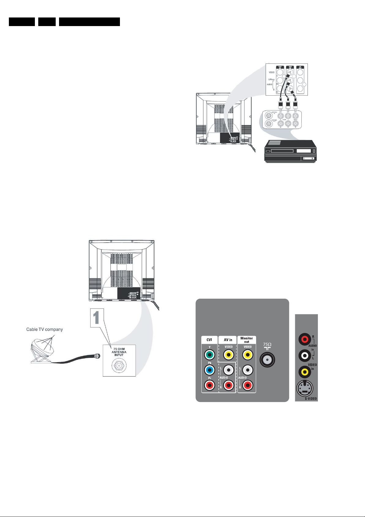
Figure 1-2 Rear audio and video connections
G_16340_002.eps
100306
1.2 Connection overview
1.2.1 Connections
G_16340_001.eps
100306
Cinch: Video CVBS - Out, Audio - Out
Ye - Video CVBS 1 V
Wh - Audio L 0.5 V
Rd - Audio R 0.5 V
/ 75 ohm kq
PP
/10 kohm kq
RMS
/ 10 kohm kq
RMS
Cinch: Video YUV- In
Gn - Video Y 1 V
Bu - Video U 0.7 V
Rd - Video V 0.7 V
/ 75 ohm jq
PP
/ 75 ohm jq
PP
/ 75 ohm jq
PP
Cinch: Audio - Out
Rd - Audio - R 0.5 V
Wh - Audio - L 0.5 V
/ 10 kohm kq
RMS
/ 10 kohm kq
RMS
Figure 1-1 Aerial connection
Aerial - In
- - F-type Coax, 75 ohm D
H_17480_008.eps
050707
Figure 1-3 Side audio and video connections
S-Video (Hosiden): Video Y/C - In
1 - Ground Y Gnd H
2 - Ground C Gnd H
3 - Video Y 1 V
4 - Video C 0.3 V
/ 75 ohm j
PP
P / 75 ohm j
PP
Cinch: Video CVBS - In, Audio - In
Ye - Video CVBS 1 V
Wh - Audio L 0.5 V
Rd - Audio R 0.5 V
/ 75 ohm jq
PP
/ 10 kohm jq
RMS
/ 10 kohm jq
RMS

Technical Specifications, Connections and Chassis Overview
1.3 Chassis Overview
See Chapter 10, Parts List.
EN 3TC5.1L CA 1.
EN 4 TC5.1L CA2.
Safety Instructions, Warnings, and Notes
2. Safety Instructions, Warnings, and Notes
Index of this chapter:
2.1 Safety Instructions
2.2 Maintenance Instructions
2.3 Warnings
2.4 Notes
2.1 Safety Instructions
Safety regulations require the following during a repair:
• Connect the set to the Mains/AC Power via an isolation
transformer (> 800 VA).
• Replace safety components, indicated by the symbol h,
only by components identical to the original ones. Any
other component substitution (other than original type) may
increase risk of fire or electrical shock hazard.
• Wear safety goggles when you replace the CRT.
Safety regulations require that after a repair, the set must be
returned in its original condition. Pay in particular attention to
the following points:
• General repair instruction: as a strict precaution, we advise
you to re-solder the solder connections through which the
horizontal deflection current flows. In particular this is valid
for the:
1. Pins of the line output transformer (LOT).
2. Fly-back capacitor(s).
3. S-correction capacitor(s).
4. Line output transistor.
5. Pins of the connector with wires to the deflection coil.
6. Other components through which the deflection current
flows.
Note: This re-soldering is advised to prevent bad connections
due to metal fatigue in solder connections, and is therefore only
necessary for television sets more than two years old.
• Route the wire trees and EHT cable correctly and secure
them with the mounted cable clamps.
• Check the insulation of the Mains/AC Power lead for
external damage.
• Check the strain relief of the Mains/AC Power cord for
proper function, to prevent the cord from touching the CRT,
hot components, or heat sinks.
• Check the electrical DC resistance between the Mains/AC
Power plug and the secondary side (only for sets that have
a Mains/AC Power isolated power supply):
1. Unplug the Mains/AC Power cord and connect a wire
between the two pins of the Mains/AC Power plug.
2. Set the Mains/AC Power switch to the "on" position
(keep the Mains/AC Power cord unplugged!).
3. Measure the resistance value between the pins of the
Mains/AC Power plug and the metal shielding of the
tuner or the aerial connection on the set. The reading
should be between 4.5 Mohm and 12 Mohm.
4. Switch "off" the set, and remove the wire between the
two pins of the Mains/AC Power plug.
• Check the cabinet for defects, to prevent touching of any
inner parts by the customer.
2.2 Maintenance Instructions
We recommend a maintenance inspection carried out by
qualified service personnel. The interval depends on the usage
conditions:
• When a customer uses the set under normal
circumstances, for example in a living room, the
recommended interval is three to five years.
• When a customer uses the set in an environment with
higher dust, grease, or moisture levels, for example in a
kitchen, the recommended interval is one year.
• The maintenance inspection includes the following actions:
1. Perform the “general repair instruction” noted above.
2. Clean the power supply and deflection circuitry on the
chassis.
3. Clean the picture tube panel and the neck of the picture
tube.
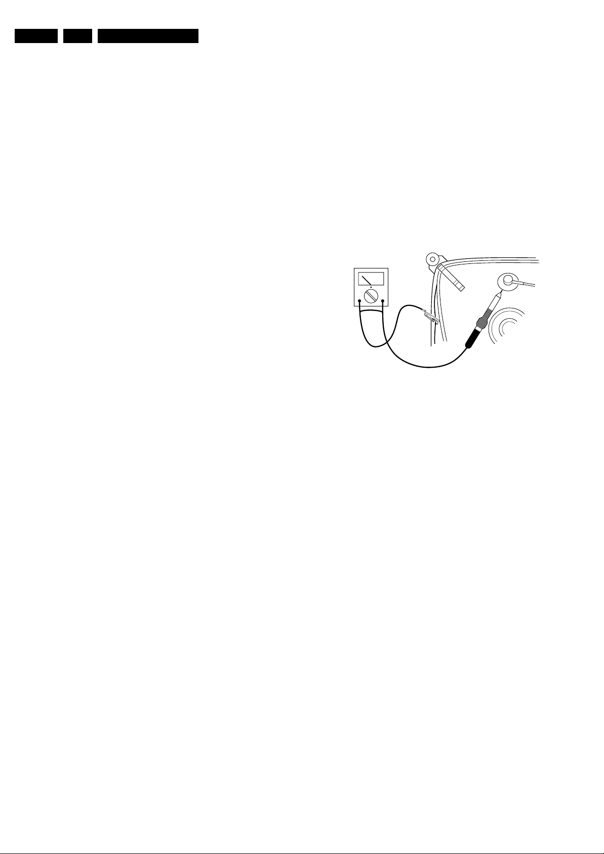
2.3 Warnings
• In order to prevent damage to ICs and transistors, avoid all
high voltage flashovers. In order to prevent damage to the
picture tube, use the method shown in figure “Discharge
picture tube”, to discharge the picture tube. Use a high
voltage probe and a multi-meter (position V
until the meter reading is 0 V (after approx. 30 s).
V
Figure 2-1 Discharge picture tube
• All ICs and many other semiconductors are susceptible to
electrostatic discharges (ESD w). Careless handling
during repair can reduce life drastically. Make sure that,
during repair, you are connected with the same potential as
the mass of the set by a wristband with resistance. Keep
components and tools also at this same potential. Available
ESD protection equipment:
– Complete kit ESD3 (small tablemat, wristband,
connection box, extension cable and earth cable) 4822
310 10671.
– Wristband tester 4822 344 13999.
• Be careful during measurements in the high voltage
section.
• Never replace modules or other components while the unit
is switched "on".
• When you align the set, use plastic rather than metal tools.
This will prevent any short circuits and prevents circuits
from becoming unstable.
2.4 Notes
2.4.1 General
• Measure the voltages and waveforms with regard to the
chassis (= tuner) ground (H), or hot ground (I), depending
on the tested area of circuitry. The voltages and waveforms
shown in the diagrams are indicative. Measure them in the
Service Default Mode (see chapter 5) with a color bar
signal and stereo sound (L: 3 kHz, R: 1 kHz unless stated
otherwise) and picture carrier at 475.25 MHz for PAL, or
61.25 MHz for NTSC (channel 3).
• Where necessary, measure the waveforms and voltages
with (D) and without (E) aerial signal. Measure the
voltages in the power supply section both in normal
operation (G) and in stand-by (F). These values are
indicated by means of the appropriate symbols.
• The semiconductors indicated in the circuit diagram and in
the parts lists, are interchangeable per position with the
). Discharge
DC
E_06532_007.eps
250304
Safety Instructions, Warnings, and Notes
EN 5TC5.1L CA 2.
semiconductors in the unit, irrespective of the type
indication on these semiconductors.
• Manufactured under license from Dolby Laboratories.
“Dolby”, “Pro Logic” and the “double-D symbol”, are
trademarks of Dolby Laboratories.
2.4.2 Schematic Notes
• All resistor values are in ohms, and the value multiplier is
often used to indicate the decimal point location (e.g. 2K2
indicates 2.2 kohm).
• Resistor values with no multiplier may be indicated with
either an "E" or an "R" (e.g. 220E or 220R indicates 220
ohm).
• All capacitor values are given in micro-farads (μ= x10
nano-farads (n= x10
• Capacitor values may also use the value multiplier as the
decimal point indication (e.g. 2p2 indicates 2.2 pF).
• An "asterisk" (*) indicates component usage varies. Refer
to the diversity tables for the correct values.
• The correct component values are listed in the Spare Parts
List. Therefore, always check this list when there is any
doubt.
2.4.3 Rework on BGA (Ball Grid Array) ICs
General
Although (LF)BGA assembly yields are very high, there may
still be a requirement for component rework. By rework, we
mean the process of removing the component from the PWB
and replacing it with a new component. If an (LF)BGA is
removed from a PWB, the solder balls of the component are
deformed drastically so the removed (LF)BGA has to be
discarded.
-9
), or pico-farads (p= x10
-12
2.4.4 Lead-free Solder
Philips CE is producing lead-free sets (PBF) from 1.1.2005
onwards.
Identification: The bottom line of a type plate gives a 14-digit
serial number. Digits 5 and 6 refer to the production year, digits
7 and 8 refer to production week (in example below it is 1991
week 18).
MODEL :
-6
),
).
PROD.NO:
Regardless of the special lead-free logo (which is not always
indicated), one must treat all sets from this date onwards
according to the rules as described below.
32PF9968/10
AG 1A0617 000001
Figure 2-2 Serial number example
MADE IN BELGIUM
220-240V 50/60Hz
~
128W
VHF+S+H+UHF
BJ3.0E LA
S
E_06532_024.eps
130606
P
b
Figure 2-3 Lead-free logo
Device Removal
As is the case with any component that is being removed, it is
essential when removing an (LF)BGA, that the board, tracks,
solder lands, or surrounding components are not damaged. To
remove an (LF)BGA, the board must be uniformly heated to a
temperature close to the reflow soldering temperature. A
uniform temperature reduces the risk of warping the PWB.
To do this, we recommend that the board is heated until it is
certain that all the joints are molten. Then carefully pull the
component off the board with a vacuum nozzle. For the
appropriate temperature profiles, see the IC data sheet.
Area Preparation
When the component has been removed, the vacant IC area
must be cleaned before replacing the (LF)BGA.
Removing an IC often leaves varying amounts of solder on the
mounting lands. This excessive solder can be removed with
either a solder sucker or solder wick. The remaining flux can be
removed with a brush and cleaning agent.
After the board is properly cleaned and inspected, apply flux on
the solder lands and on the connection balls of the (LF)BGA.
Note: Do not apply solder paste, as this has been shown to
result in problems during re-soldering.
Device Replacement
The last step in the repair process is to solder the new
component on the board. Ideally, the (LF)BGA should be
aligned under a microscope or magnifying glass. If this is not
possible, try to align the (LF)BGA with any board markers.
So as not to damage neighboring components, it may be
necessary to reduce some temperatures and times.
More Information
For more information on how to handle BGA devices, visit this
URL: www.atyourservice.ce.philips.com (needs subscription,
not available for all regions). After login, select “Magazine”,
then go to “Repair downloads”. Here you will find Information
on how to deal with BGA-ICs.
Due to lead-free technology some rules have to be respected
by the workshop during a repair:
• Use only lead-free soldering tin Philips SAC305 with order
code 0622 149 00106. If lead-free solder paste is required,
please contact the manufacturer of your soldering
equipment. In general, use of solder paste within
workshops should be avoided because paste is not easy to
store and to handle.
• Use only adequate solder tools applicable for lead-free
soldering tin. The solder tool must be able:
– To reach a solder-tip temperature of at least 400°C.
– To stabilize the adjusted temperature at the solder-tip.
– To exchange solder-tips for different applications.
• Adjust your solder tool so that a temperature of around
360°C - 380°C is reached and stabilized at the solder joint.
Heating time of the solder-joint should not exceed ~ 4 sec.
Avoid temperatures above 400°C, otherwise wear-out of
tips will increase drastically and flux-fluid will be destroyed.
To avoid wear-out of tips, switch “off” unused equipment or
reduce heat.
• Mix of lead-free soldering tin/parts with leaded soldering
tin/parts is possible but PHILIPS recommends strongly to
avoid mixed regimes. If this cannot be avoided, carefully
clean the solder-joint from old tin and re-solder with new
tin.
• Use only original spare-parts listed in the Service-Manuals.
Not listed standard material (commodities) has to be
purchased at external companies.
• Special information for lead-free BGA ICs: these ICs will be
delivered in so-called "dry-packaging" to protect the IC
against moisture. This packaging may only be opened
shortly before it is used (soldered). Otherwise the body of
the IC gets "wet" inside and during the heating time the
structure of the IC will be destroyed due to high (steam-)
pressure inside the body. If the packaging was opened
before usage, the IC has to be heated up for some hours
(around 90°C) for drying (think of ESD-protection!).
Do not re-use BGAs at all!

EN 6 TC5.1L CA3.
Directions for Use
• For sets produced before 1.1.2005, containing leaded
soldering tin and components, all needed spare parts will
be available till the end of the service period. For the repair
of such sets nothing changes.
In case of doubt whether the board is lead-free or not (or with
mixed technologies), you can use the following method:
• Always use the highest temperature to solder, when using
SAC305 (see also instructions below).
• De-solder thoroughly (clean solder joints to avoid mix of
two alloys).
Caution: For BGA-ICs, you must use the correct temperatureprofile, which is coupled to the 12NC. For an overview of these
profiles, visit the website www.atyourservice.ce.philips.com
(needs subscription, but is not available for all regions)
You will find this and more technical information within the
"Magazine", chapter "Repair downloads".
For additional questions please contact your local repair help
desk.
2.4.5 Alternative BOM identification
In September 2003, Philips CE introduced a change in the way
the serial number (or production number, see Figure 2-1) is
composed. From this date on, the third digit in the serial
number (example: AG2B0335000001) indicates the number of
the alternative BOM (Bill of Materials used for producing the
specific model of TV set). It is possible that the same TV model
on the market is produced with e.g. two different types of
displays, coming from two different O.E.M.s.
By looking at the third digit of the serial number, the service
technician can see if there is more than one type of B.O.M.
used in the production of the TV set he is working with. He can
then consult the At Your Service Web site, where he can type
in the Commercial Type Version Number of the TV set (e.g.
28PW9515/12), after which a screen will appear that gives
information about the number of alternative B.O.M.s used.
If the third digit of the serial number contains the number 1
(example: AG1B033500001), then there is only one B.O.M.
version of the TV set on the market. If the third digit is a 2
(example: AG2B0335000001), then there are two different
B.O.M.s. Information about this is important for ordering the
correct spare parts!
For the third digit, the numbers 1...9 and the characters A...Z
can be used, so in total: 9 plus 26 = 35 different B.O.M.s can
be indicated by the third digit of the serial number.
2.4.6 Practical Service Precautions
• It makes sense to avoid exposure to electrical shock.
While some sources are expected to have a possible
dangerous impact, others of quite high potential are of
limited current and are sometimes held in less regard.
• Always respect voltages. While some may not be
dangerous in themselves, they can cause unexpected
reactions that are best avoided. Before reaching into a
powered TV set, it is best to test the high voltage insulation.
It is easy to do, and is a good service precaution.
3. Directions for Use
You can download this information from the following websites:
http://www.philips.com/support
http://www.p4c.philips.com
4. Mechanical Instructions
See Chapter 10, Parts List.
Service Modes, Error Codes, and Fault Finding
5. Service Modes, Error Codes, and Fault Finding
5.1 Trouble Shooting
5.1.1 Can not Power On
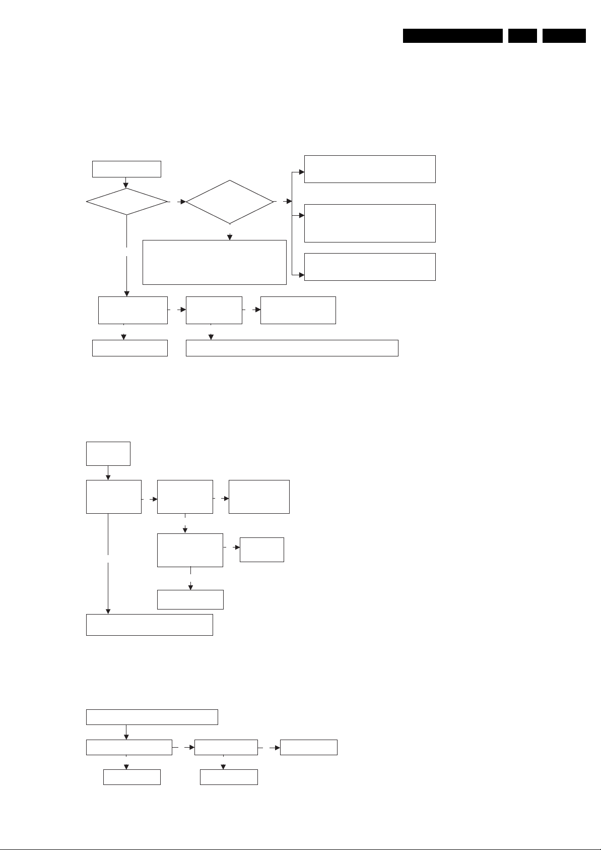
EN 7TC5.1L CA 5.
Can not Power On
Fuse OK?
(1) Check if B+ shorted to earth.
(2) To check whether D822 and R821 are
N
(3) To check whether D823 and R823 are
Is it IC801 Pin 1
shorted to earth?
Y
Check/Replace IC801
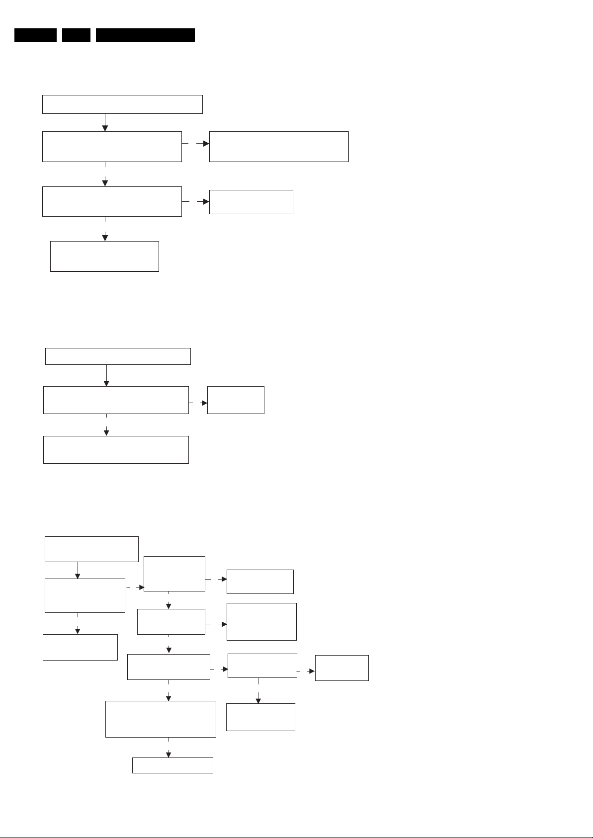
5.1.2 No Raster, Sound OK
No Raster
Sound OK
Check B+,
Y Y
turnoff.
turnoff. And whether C836 shorted.
+12V, Ok?
N
Is DB801 OK?
NN
Y
Check the components such as C801, C802, C806, C807 and C815
Is power supply for IC101 correct?
If not, check Q820, Q821, Q007, Q008,
D001
Check Horizontal Scan circuit:
Check H-Vcc and H-out of IC 101
Check Q401, T401 and Q411
Check standby circuit: Check Pin64 of
IC101, Check Q825, Q824, Q823, Q822.
Replace DB801
Figure 5-1 Can not Power On
G_16340_004.eps
100306
Is the power
supply of Q401
and Q411 ok?
N
To check whether R404, C401, T401,
Q401, R422 are ok?
Check Pin 13
(H-OUT) voltage
ok?
Y
Is there any shorted
in the scan part of
the circuit?
Change IC101
Y
N
Y
N
5.1.3 Raster OK, Sound OK, No TV/AV picture
Raster OK, Sound OK, No TV/AV picture
Check whether Q917 is
ok?
N
Replace Q917
Y Y
Replace C238
N
Check each
output voltage of
FBT
Change the
shorted part.
G_16340_005.eps
100306
Figure 5-2 No Raster, Sound OK
Change IC901 Check C238, ok?
G_16340_008.eps
100306
Figure 5-3 Raster OK, Sound OK, No TV/AV picture
EN 8 TC5.1L CA5.
5.1.4 Raster OK, Sound OK, No AV picture
Raster OK, Sound OK, No AV picture
Service Modes, Error Codes, and Fault Finding
Is the signal waveform at Pin 12 and
Pin 14 of IC901 right?
Y
Check Q917, Q918, Q919, ok?
N
Replace the fail component.
5.1.5 Raster OK, Sound OK, No TV picture
Raster OK, Sound OK, No TV picture
Is the signal waveform at Pin 15 of IC901
right?
N
To check whether R903, C903, R902
N
and R905, C908, R908 are ok?
Replace IC901
Y
G_16340_006.eps
100306
Figure 5-4 Raster OK, Sound OK, No AV picture
Replace
IC901
Y
Check R234, Q204, R235, C229
5.1.6 No picture, dense noise dots
No picture, dense noise
dots
Is the antenna feed line
or the adapter broken?
Y
Handing the antenna
fault
N
Is the signal at Pin SCL,
SDA of tuner ok?
Check signal at P5, P57, P58,
P59, and P60 of IC101 and
replace the abnormal relative
circuit
Figure 5-5 Raster OK, Sound OK, No TV picture
Is the signal at
Pin41, Pin42 of
IC101 ok?
N
Is the signal at IF
pin of the tuner ok?
N
N N
Y
G_16340_007.eps
Check/Replace
Y
IC101
Check the relative
circuit of Q101,
Y
Z141 etc
Is the supply
voltage of tuner ok?
Y
Check/Replace
IC201, IC202,
D101.
100306
Check/Replace
Tuner
Y
Check EEPROM
G_16340_009.eps
Figure 5-6 No picture, dense noise dots
100306
 Loading...