

Philips TC5.1L Service Manual
Color Television Chassis
TC5.1L
CB
H_17510_000.eps
021107
Contents Page
1. Technical Specifications, Connections and Chassis
Overview 2
2. Safety Instructions, Warnings, and Notes 4
3. Directions for Use 6
4. Mechanical Instructions 6
5. Service Modes, Error Codes, and Fault Finding 7
6. Block Diagrams, Test Point Overviews, and
Waveforms
Chassis Block Diagram 9
7. Circuit Diagrams and CBA Layouts Diagram CBA
Main Board 01-29PT6457/44-MA1 10 12
Main Board 01-29PT6457/55-MA1 11 12
CRT Panel 13 14
Side I/O Panel 40-TB59PH-SIA1XG 14
Layout Front IR Panel 40-TB59PH-FBB1XG 14
Technical Specifications, Connections and Chassis Overview
EN 2 TC5.1L CB1.
1. Technical Specifications, Connections and Chassis Overview
1.1 Technical Specifications
Tuning - technology : PLL
Tuning - presets/channels : 181
Freq Bands : Full-Cable
TV Systems Off Air/ Cable : NTSC M (3.58 - 4.5)
TV Systems Multi : NTSC
Mains voltage : 180-240V
(29PT6457/44)
: 100-120V
: (29PT6457/55)
Mains frequency : 50/60Hz
Power consumption : 90W (29PT6457/44)
: 95W (29PT6457/55)
Standby Power consumption : <3W (29PT6457/44)
: <1W (29PT6457/55)
Sound Systems : BTCS SAP
Audio output (RMS) : 2x5W
Scan Modes : 4:3
Sound Features : AVL, Mute
Sound Control : 4 sound modes
: Balance
: Bass Boost
: Treble Boost,
: Volume
Menu Languages : American English,
French, Spanish
Clock/Timer Function : Sleep timer
Terrestrial Antenna in : 75 Ohm (F type)
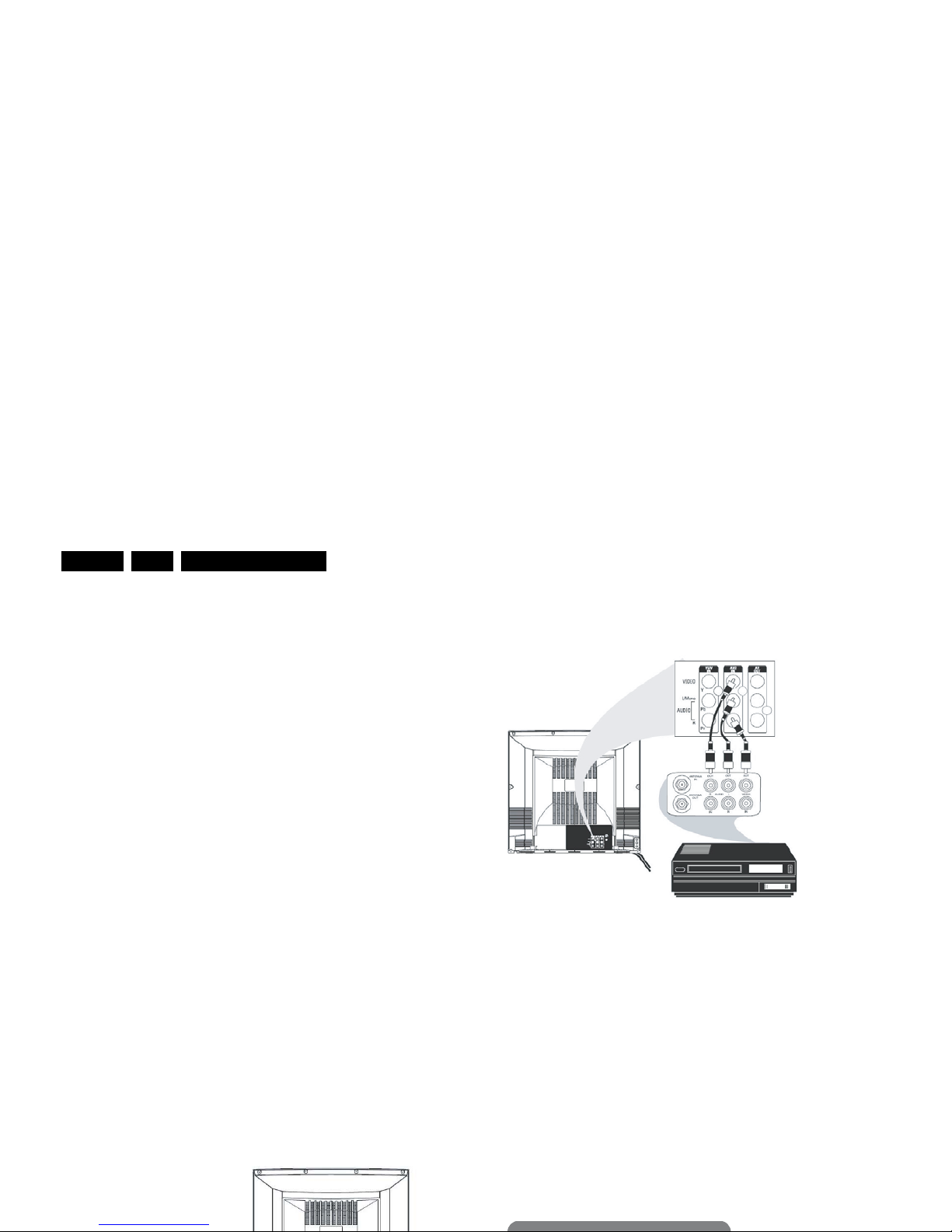
1.2 Connection overview
1.2.1 Connections
Figure 1-2 Rear audio and video connections
Cinch: Video CVBS - Out, Audio - Out
Ye - Video CVBS 1 V
PP
/ 75 ohm kq
Wh - Audio L 0.5 V
RMS
/10 kohm kq
Rd - Audio R 0.5 V
RMS
/ 10 kohm kq
Cinch: Video YUV- In
Gn - Video Y 1 V
PP
/ 75 ohm jq
Bu - Video U 0.7 V
PP
/ 75 ohm jq
Rd - Video V 0.7 V
PP
/ 75 ohm jq
Cinch: Audio - Out
Rd - Audio - R 0.5 V
RMS
/ 10 kohm kq
Wh - Audio - L 0.5 V
RMS
/ 10 kohm kq
G_16340_002.eps
100306

Technical Specifications, Connections and Chassis Overview
EN 3TC5.1L CB 1.
1.3 Chassis Overview
See Chapter 10, Parts List.
Safety Instructions, Warnings, and Notes
EN 4 TC5.1L CB2.
2. Safety Instructions, Warnings, and Notes
Index of this chapter:
2.1 Safety Instructions
2.2 Maintenance Instructions
2.3 Warnings
2.4 Notes
2.1 Safety Instructions
Safety regulations require the following during a repair:
• Connect the set to the Mains/AC Power via an isolation
transformer (> 800 VA).
• Replace safety components, indicated by the symbol h,
only by components identical to the original ones. Any
other component substitution (other than original type) may
increase risk of fire or electrical shock hazard.
• Wear safety goggles when you replace the CRT.
Safety regulations require that after a repair, the set must be
returned in its original condition. Pay in particular attention to
the following points:
• General repair instruction: as a strict precaution, we advise
you to re-solder the solder connections through which the
horizontal deflection current flows. In particular this is valid
for the:
1. Pins of the line output transformer (LOT).
2. Fly-back capacitor(s).
3. S-correction capacitor(s).
4. Line output transistor.
5. Pins of the connector with wires to the deflection coil.
6. Other components through which the deflection current
flows.
Note: This re-soldering is advised to prevent bad connections
due to metal fatigue in solder connections, and is therefore only
necessary for television sets more than two years old.
• Route the wire trees and EHT cable correctly and secure
them with the mounted cable clamps.
• Check the insulation of the Mains/AC Power lead for
external damage.
• Check the strain relief of the Mains/AC Power cord for
1. Perform the “general repair instruction” noted above.
2. Clean the power supply and deflection circuitry on the
chassis.
3. Clean the picture tube panel and the neck of the picture
tube.
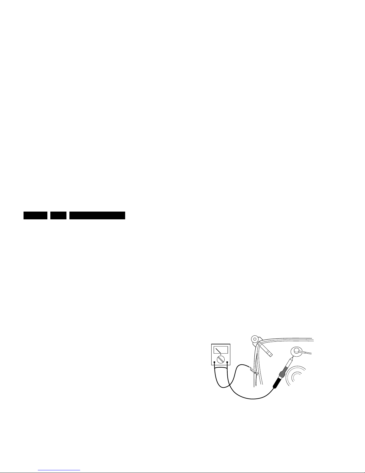
2.3 Warnings
• In order to prevent damage to ICs and transistors, avoid all
high voltage flashovers. In order to prevent damage to the
picture tube, use the method shown in figure “Discharge
picture tube”, to discharge the picture tube. Use a high
voltage probe and a multi-meter (position V
DC
). Discharge
until the meter reading is 0 V (after approx. 30 s).
Figure 2-1 Discharge picture tube
• All ICs and many other semiconductors are susceptible to
electrostatic discharges (ESD w). Careless handling
during repair can reduce life drastically. Make sure that,
during repair, you are connected with the same potential as
the mass of the set by a wristband with resistance. Keep
components and tools also at this same potential. Available
ESD protection equipment:
– Complete kit ESD3 (small tablemat, wristband,
connection box, extension cable and earth cable) 4822
V
E_06532_007.eps
250304
Safety Instructions, Warnings, and Notes
EN 5TC5.1L CB 2.
semiconductors in the unit, irrespective of the type
indication on these semiconductors.
• Manufactured under license from Dolby Laboratories.
“Dolby”, “Pro Logic” and the “double-D symbol”, are
trademarks of Dolby Laboratories.
2.4.2 Schematic Notes
• All resistor values are in ohms, and the value multiplier is
often used to indicate the decimal point location (e.g. 2K2
indicates 2.2 kohm).
• Resistor values with no multiplier may be indicated with
either an "E" or an "R" (e.g. 220E or 220R indicates 220
ohm).
• All capacitor values are given in micro-farads (μ= x10
-6
),
nano-farads (n= x10
-9
), or pico-farads (p= x10
-12
).
• Capacitor values may also use the value multiplier as the
decimal point indication (e.g. 2p2 indicates 2.2 pF).
• An "asterisk" (*) indicates component usage varies. Refer
to the diversity tables for the correct values.
• The correct component values are listed in the Spare Parts
List. Therefore, always check this list when there is any
doubt.
2.4.3 Rework on BGA (Ball Grid Array) ICs
General
Although (LF)BGA assembly yields are very high, there may
still be a requirement for component rework. By rework, we
mean the process of removing the component from the PWB
and replacing it with a new component. If an (LF)BGA is
removed from a PWB, the solder balls of the component are
deformed drastically so the removed (LF)BGA has to be
discarded.
Device Removal
As is the case with any component that is being removed, it is
essential when removing an (LF)BGA, that the board, tracks,
solder lands, or surrounding components are not damaged. To
remove an (LF)BGA, the board must be uniformly heated to a
temperature close to the reflow soldering temperature. A
uniform temperature reduces the risk of warping the PWB.
To do this, we recommend that the board is heated until it is
2.4.4 Lead-free Solder
Philips CE is producing lead-free sets (PBF) from 1.1.2005
onwards.
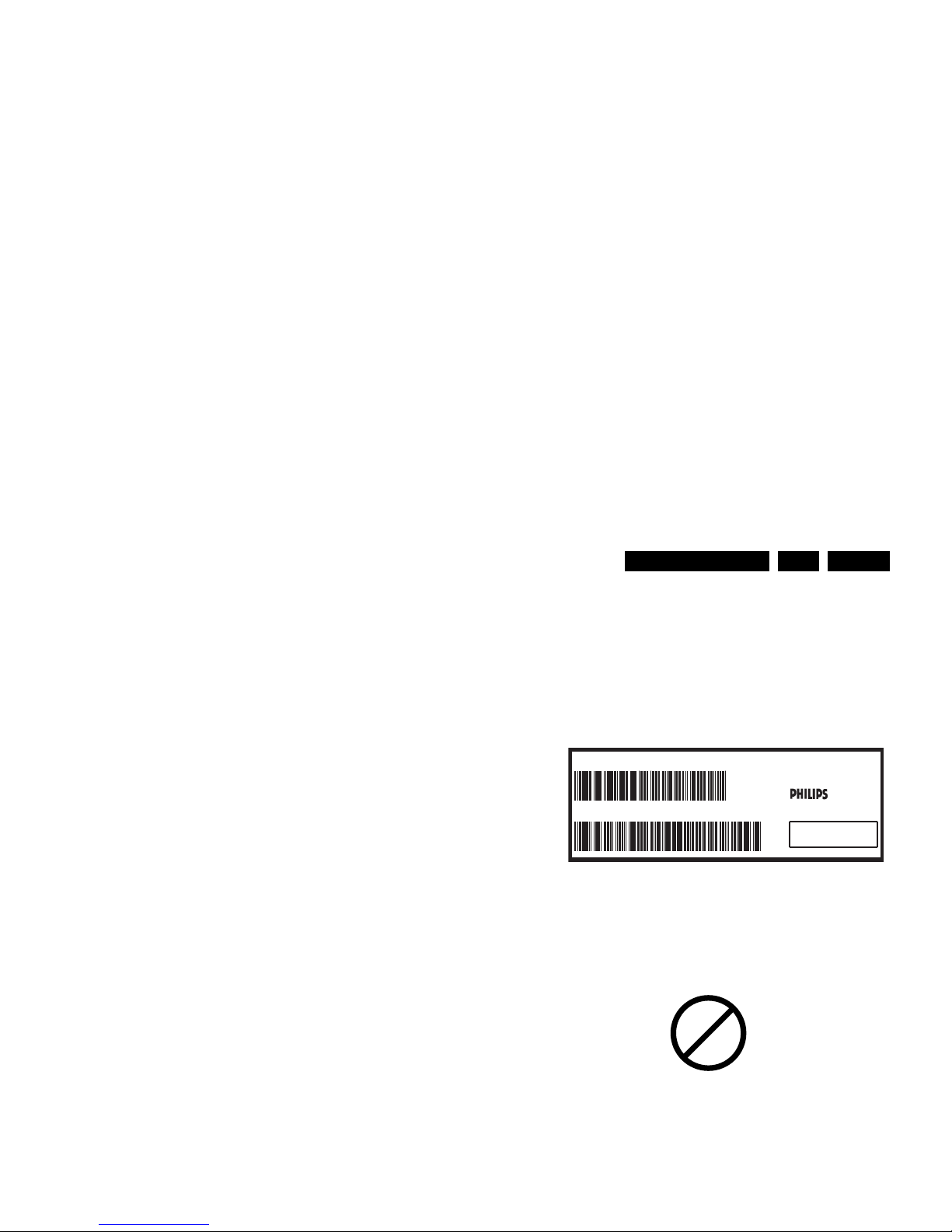
Identification: The bottom line of a type plate gives a 14-digit
serial number. Digits 5 and 6 refer to the production year, digits
7 and 8 refer to production week (in example below it is 1991
week 18).
Figure 2-2 Serial number example
Regardless of the special lead-free logo (which is not always
indicated), one must treat all sets from this date onwards
according to the rules as described below.
Figure 2-3 Lead-free logo
Due to lead-free technology some rules have to be respected
by the workshop during a repair:
• Use only lead-free soldering tin Philips SAC305 with order
code 0622 149 00106. If lead-free solder paste is required,
please contact the manufacturer of your soldering
equipment. In general, use of solder paste within
workshops should be avoided because paste is not easy to
E_06532_024.eps
130606
MODEL :
PROD.NO:
~
S
32PF9968/10
MADE IN BELGIUM
220-240V 50/60Hz
128W
AG 1A0617 000001
VHF+S+H+UHF
BJ3.0E LA
P
b

Directions for Use
EN 6 TC5.1L CB3.
• For sets produced before 1.1.2005, containing leaded
soldering tin and components, all needed spare parts will
be available till the end of the service period. For the repair
of such sets nothing changes.
In case of doubt whether the board is lead-free or not (or with
mixed technologies), you can use the following method:
• Always use the highest temperature to solder, when using
SAC305 (see also instructions below).
• De-solder thoroughly (clean solder joints to avoid mix of
two alloys).
Caution: For BGA-ICs, you must use the correct temperatureprofile, which is coupled to the 12NC. For an overview of these
profiles, visit the website www.atyourservice.ce.philips.com
(needs subscription, but is not available for all regions)
You will find this and more technical information within the
"Magazine", chapter "Repair downloads".
For additional questions please contact your local repair help
desk.
2.4.5 Alternative BOM identification
In September 2003, Philips CE introduced a change in the way
the serial number (or production number, see Figure 2-1) is
composed. From this date on, the third digit in the serial
number (example: AG2B0335000001) indicates the number of
the alternative BOM (Bill of Materials used for producing the
specific model of TV set). It is possible that the same TV model
on the market is produced with e.g. two different types of
displays, coming from two different O.E.M.s.
By looking at the third digit of the serial number, the service
technician can see if there is more than one type of B.O.M.
used in the production of the TV set he is working with. He can
then consult the At Your Service Web site, where he can type
in the Commercial Type Version Number of the TV set (e.g.
28PW9515/12), after which a screen will appear that gives
information about the number of alternative B.O.M.s used.
If the third digit of the serial number contains the number 1
(example: AG1B033500001), then there is only one B.O.M.
version of the TV set on the market. If the third digit is a 2
(example: AG2B0335000001), then there are two different
B.O.M.s. Information about this is important for ordering the
correct spare parts!
For the third digit, the numbers 1...9 and the characters A...Z
can be used, so in total: 9 plus 26 = 35 different B.O.M.s can
be indicated by the third digit of the serial number.
2.4.6 Practical Service Precautions
• It makes sense to avoid exposure to electrical shock.
While some sources are expected to have a possible
dangerous impact, others of quite high potential are of
limited current and are sometimes held in less regard.
• Always respect voltages. While some may not be
dangerous in themselves, they can cause unexpected
reactions that are best avoided. Before reaching into a
powered TV set, it is best to test the high voltage insulation.
It is easy to do, and is a good service precaution.
3. Directions for Use
You can download this information from the following websites:
http://www.philips.com/support
http://www.p4c.philips.com
Service Modes, Error Codes, and Fault Finding
EN 7TC5.1L CB 5.
5. Service Modes, Error Codes, and Fault Finding
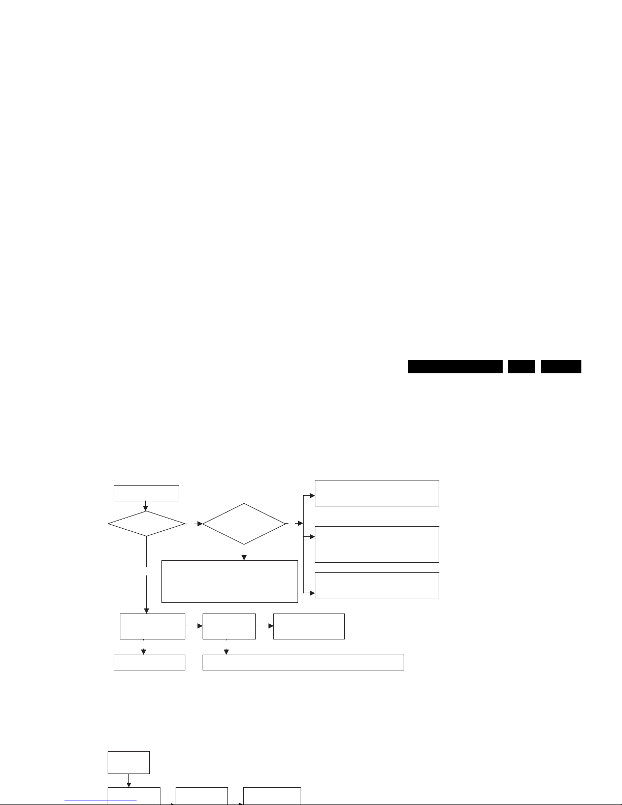
5.1 Trouble Shooting
5.1.1 Can not Power On
Figure 5-1 Can not Power On
5.1.2 No Raster, Sound OK
G_16340_004.eps
100306
Can not Power On
Fuse OK?
Check B+,
+12V, Ok?
Is power supply for IC101 correct?
If not, check Q820, Q821, Q007, Q008,
D001
Check standby circuit: Check Pin64 of
IC101, Check Q825, Q824, Q823, Q822.
Check Horizontal Scan circuit:
Check H-Vcc and H-out of IC 101
Check Q401, T401 and Q411
(1) Check if B+ shorted to earth.
(2) To check whether D822 and R821 are
turnoff.
(3) To check whether D823 and R823 are
turnoff. And whether C836 shorted.
Is it IC801 Pin 1
shorted to earth?
Is DB801 OK?
Check the components such as C801, C802, C806, C807 and C815
Replace DB801
Check/Replace IC801
Y Y
Y
NN
N
N
Y
Is the power
supply of Q401
Check Pin 13
(H-OUT) voltage
Check each
output voltage of
No Raster
Sound OK
Service Modes, Error Codes, and Fault Finding
EN 8 TC5.1L CB5.
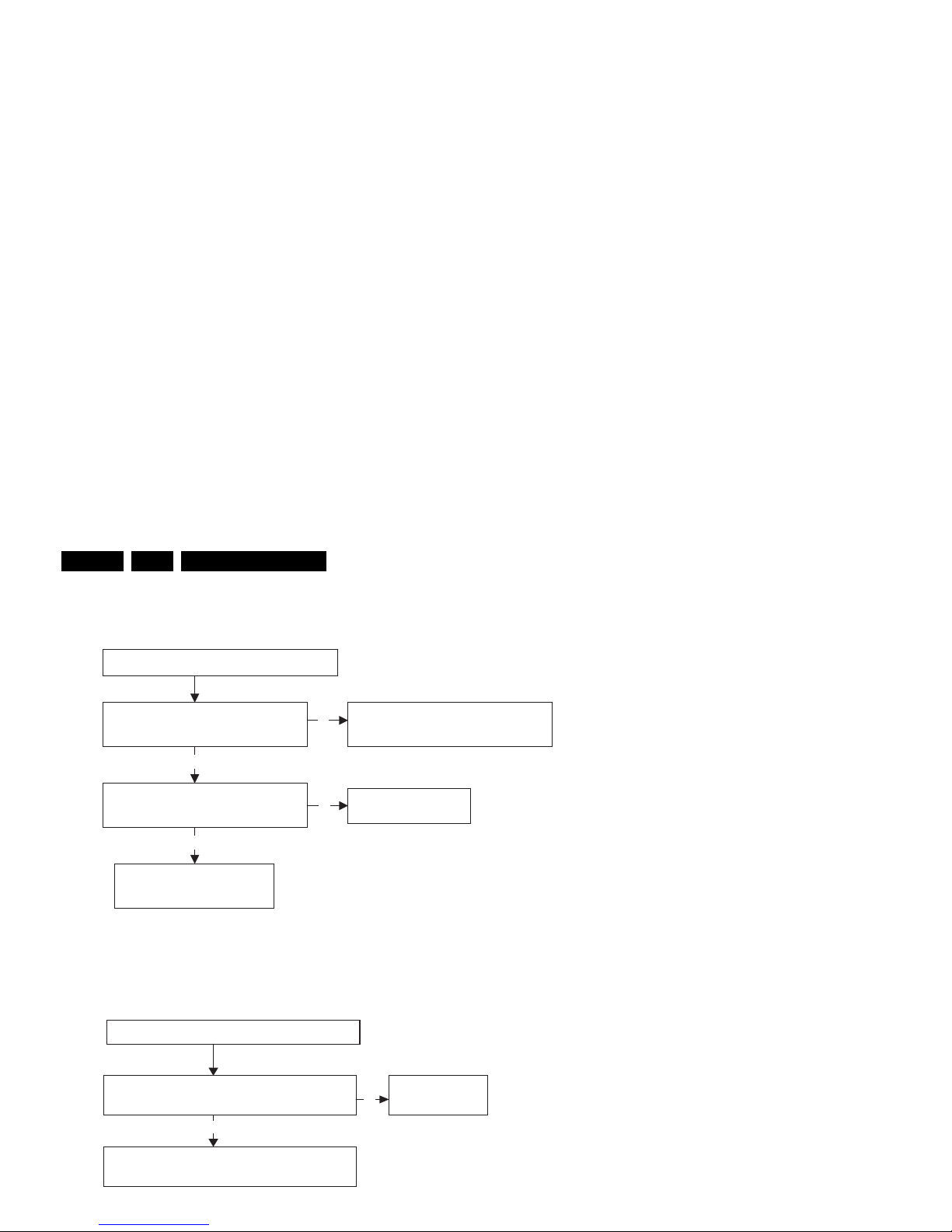
5.1.4 Raster OK, Sound OK, No AV picture
Figure 5-4 Raster OK, Sound OK, No AV picture
5.1.5 Raster OK, Sound OK, No TV picture
Figure 5-5 Raster OK, Sound OK, No TV picture
G_16340_006.eps
100306
To check whether R903, C903, R902
and R905, C908, R908 are ok?
Is the signal waveform at Pin 12 and
Pin 14 of IC901 right?
Raster OK, Sound OK, No AV picture
Replace IC901
Check Q917, Q918, Q919, ok?
Replace the fail component.
Y
N
N
Y
G_16340_007.eps
100306
Replace
IC901
Is the signal waveform at Pin 15 of IC901
right?
Raster OK, Sound OK, No TV picture
Check R234, Q204, R235, C229
N
Y
Block Diagrams, Test Point Overviews, and Waveforms
EN 9TC5.1L CB 6.
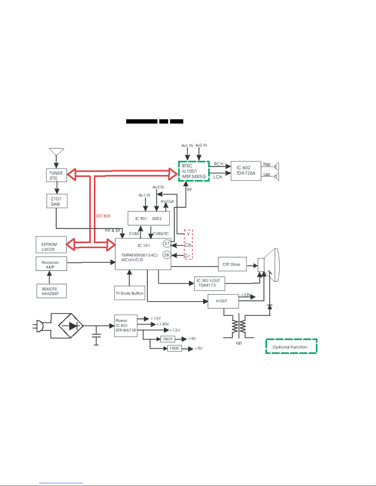
6. Block Diagrams, Test Point Overviews, and Waveforms
Chassis Block Diagram
H_17510_009.eps
021107
* /44 sets use STR-W6756
 Loading...